
Method for growth of SiC crystal for off-axis substrate and method for preparing N type SiC substrate with high electric uniformity
A growth method and substrate technology, applied in the directions of crystal growth, single crystal growth, single crystal growth, etc., can solve problems such as difficult to meet high-performance power devices, and achieve the effect of reducing defect density and improving resistivity uniformity
Patent Information
- Authority / Receiving Office
- CN · China
- Current Assignee / Owner
- Publication Date
- 2016-10-12
Smart Images
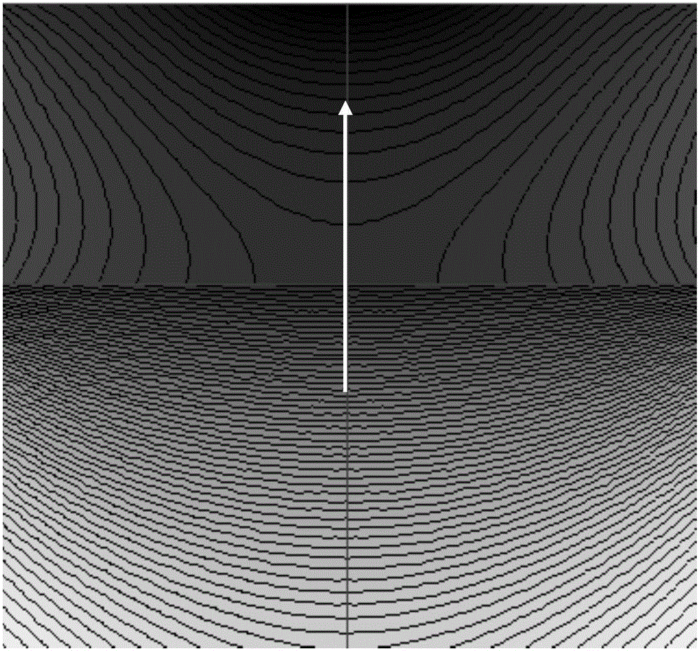
Figure 1 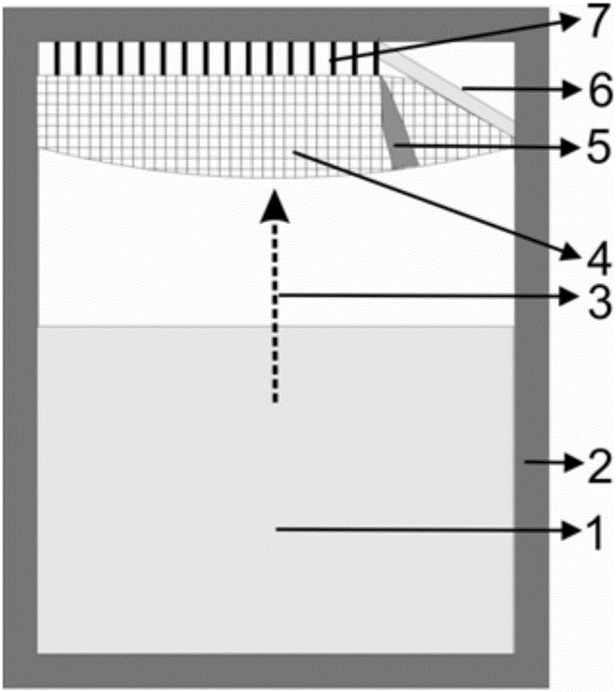
Figure 2 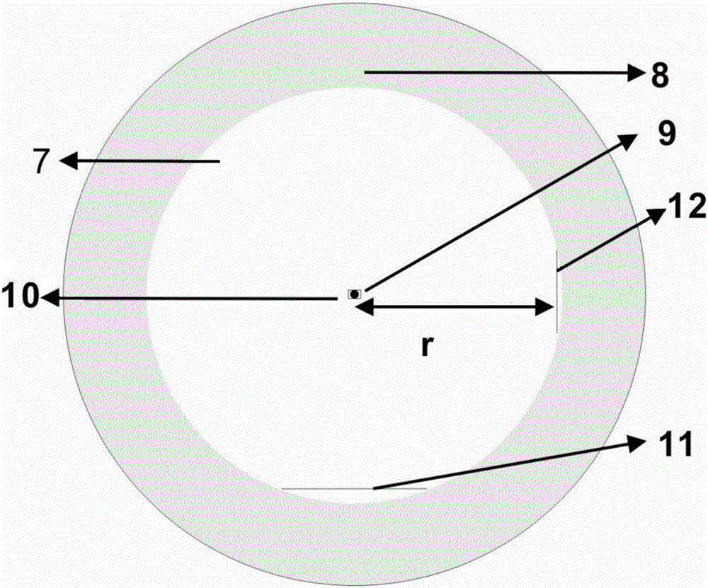
Figure 3
Abstract
Description
technical field
[0001] The invention relates to the growth of SiC crystals for off-axis substrates and a method for preparing N-type SiC single crystal substrates with low defect density and high electrical uniformity, belonging to the technical field of crystal growth. Background technique
[0002] Silicon carbide is the representative of the third generation of wide bandgap semiconductors. It has excellent electrical and thermal properties such as large bandgap, high mobility, and high thermal conductivity. It has become an ideal material for making high-frequency, high-power, high-temperature and radiation-resistant devices. In terms of device development, silicon carbide blue LEDs have been commercialized; research and development of silicon carbide power devices has become the mainstream of research and development of new power semiconductor devices; see CN104246979A "High-voltage semiconductor devices on SiC". In terms of high-temperature semiconductor devices, silicon...
Examples
Embodiment 1
[0039] The growth device used in Example 1 is a single crystal growth furnace, including a growth chamber, a graphite crucible, an insulating material and an induction heating system. There is a water cooling device on the side wall of the growth chamber, and the water cooling device is a sealed double-layer tube made of quartz glass. The circulating working medium in the tube is water, and the water temperature is kept constant during the growth process; the seed crystal is fixed on the graphite upper cover; the crucible and insulation material are placed in the growth chamber, and the growth chamber can reach 1×10 -6 Vacuum above mbar. Regarding the growth device, refer to Example 1 of CN1554808A, and the parts that are not inconsistent with the present invention are included in the present invention by reference.
[0040] As a comparative example, the traditional symmetric bonded seed crystal is shown as image 3 As shown, a 4-inch (r=50mm) SiC seed crystal 7 is symmetrica...
Embodiment 2
[0046] Example 2: Preparation of 4-inch 4° N-type SiC substrate
[0047] 1. The SiC crystal with a diameter of 120 mm obtained in Example 1 is subjected to rounding processing, and the small face and the junction area growing outward along the small side of the seed crystal are removed, so that the diameter of the SiC single crystal rod is 100 mm,
[0048] 2. Cut, grind and polish the SiC single crystal rod with a diameter of 100 mm to obtain a 4° N-type SiC substrate. Figure 7 , Figure 8 It is a photo of the fabricated 4° N-type SiC substrate material, numbered wafer 06 and wafer 20 respectively.
[0049] The partial 4° N-type SiC substrates numbered wafer 06 and wafer 20 were taken to test the resistivity. The results are as follows: there is still a residual small area on the far right side of wafer 06, the maximum resistivity is 0.01792 ohm*cm, and the minimum The value is 0.01735 ohm*cm with a deviation of 3.1%. However, the facet area of the wafer 20 has been comp...