
A lateral double-diffusion mos device
A MOS device, lateral double diffusion technology, applied in semiconductor devices, electrical components, circuits, etc., can solve the problems of substrate depletion, substrate-assisted depletion, superjunction LDMOS effect, etc., to achieve uniform electric field distribution, The effect of increasing the reverse blocking voltage
Patent Information
- Authority / Receiving Office
- CN · China
- Patent Type
- Patents(China)
- Current Assignee / Owner
- Publication Date
- 2020-03-31
Smart Images
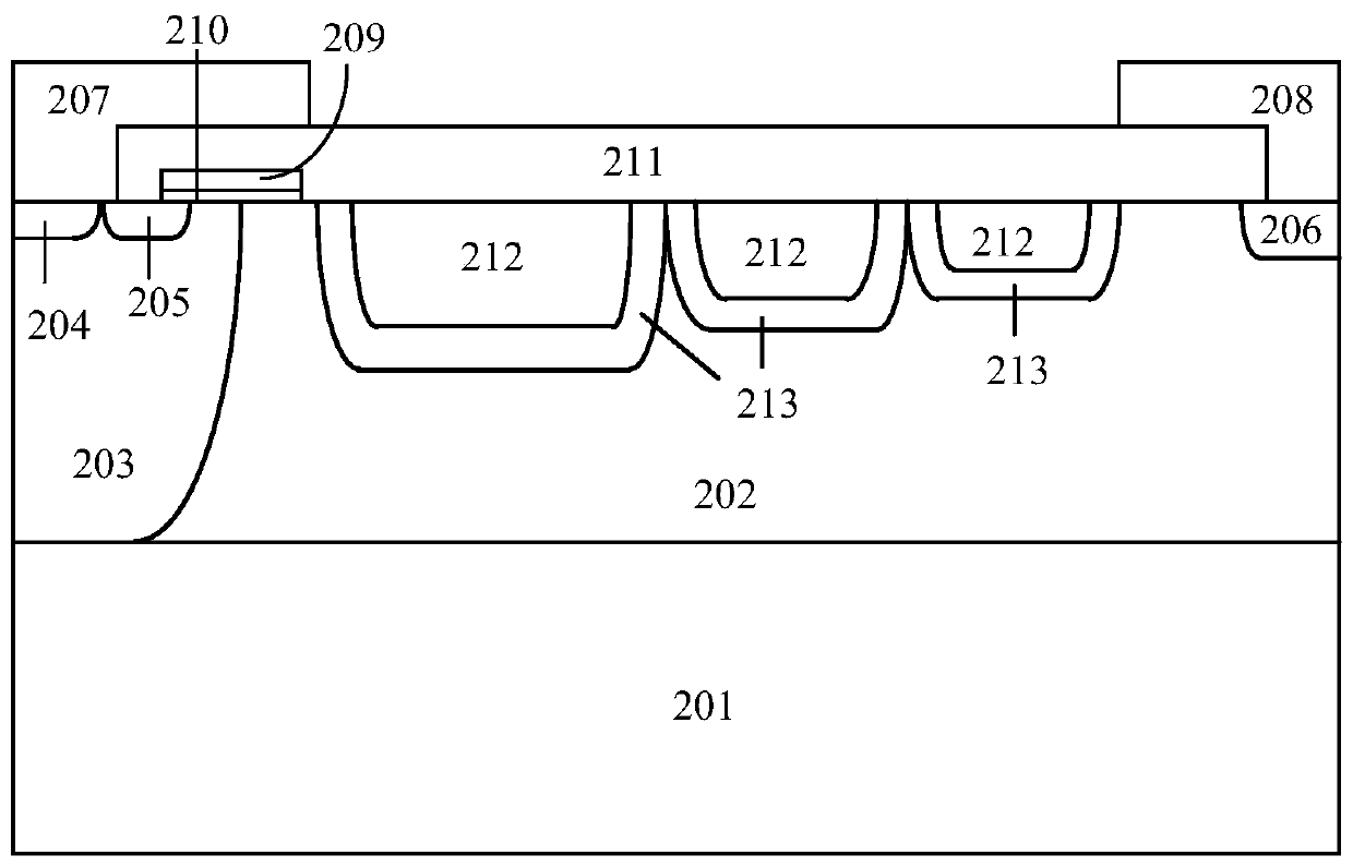
Figure 1
Abstract
Description
technical field
[0001] The invention relates to the technical field of semiconductor devices, in particular to a lateral double-diffusion MOS device. Background technique
[0002] Metal oxide power MOS semiconductor devices, with the rapid development of the semiconductor industry, power electronics technology represented by high-power semiconductor devices has developed rapidly, and its application fields have continued to expand, such as the control of AC motors and printer drive circuits. Among various power devices today, laterally diffused MOS devices (LDMOS) have the advantages of high operating voltage and easy integration, so they are widely used.
[0003] In the design of LDMOS devices, the breakdown voltage and on-resistance have always been the main goals that people pay attention to when designing such devices. The thickness of the epitaxial layer, doping concentration, and the length of the drift region are the most important parameters of LDMOS. The traditiona...
Examples
Embodiment 1
[0016] In this embodiment, the semiconductor of the first conductivity type is a P-type semiconductor, the semiconductor of the second conductivity type is an N-type semiconductor, and the charges stored in the polysilicon island 212 are negative charges.
[0017] A kind of lateral double diffusion MOS device, comprises P-type semiconductor substrate 201 and the P-type semiconductor body region 203 and N-type semiconductor drift region 202 that are arranged on the upper surface of P-type semiconductor substrate 201, P-type semiconductor body region 203 and N-type The semiconductor drift region 202 is side contacted; the inner upper surface of the P-type semiconductor body region 203 has an N-type semiconductor source region 205 and a highly doped P-type semiconductor body contact region 204; the N-type semiconductor source region 205 and the highly doped P The P-type semiconductor body contact region 204 is in direct contact with the metal source 207 located on its upper surfac...
Embodiment 2
[0023] In this embodiment, the semiconductor of the first conductivity type is an N-type semiconductor, the semiconductor of the second conductivity type is a P-type semiconductor, and the charges stored in the polysilicon island 212 are positive charges.
[0024]A lateral double-diffused MOS device, comprising an N-type semiconductor substrate 201 and an N-type semiconductor body region 203 and a P-type semiconductor drift region 202 arranged on the upper surface of the N-type semiconductor substrate 201, and an N-type semiconductor body region 203 and a P-type semiconductor region. The semiconductor drift region 202 is side contacted; the upper surface of the N-type semiconductor body region 203 has a P-type semiconductor source region 205 and a highly doped N-type semiconductor body contact region 204; the P-type semiconductor source region 205 and the highly doped N The N-type semiconductor body contact region 204 is in direct contact with the metal source 207 located on it...