
LED chip and manufacturing method thereof
A technology of LED chips and manufacturing methods, which is applied to electrical components, circuits, semiconductor devices, etc., can solve problems such as insufficient brightness of light-emitting diodes, and achieve the effects of high production efficiency, convenient operation, and simple manufacturing methods
Patent Information
- Authority / Receiving Office
- CN · China
- Patent Type
- Applications(China)
- Current Assignee / Owner
- Publication Date
- 2018-06-19
Smart Images
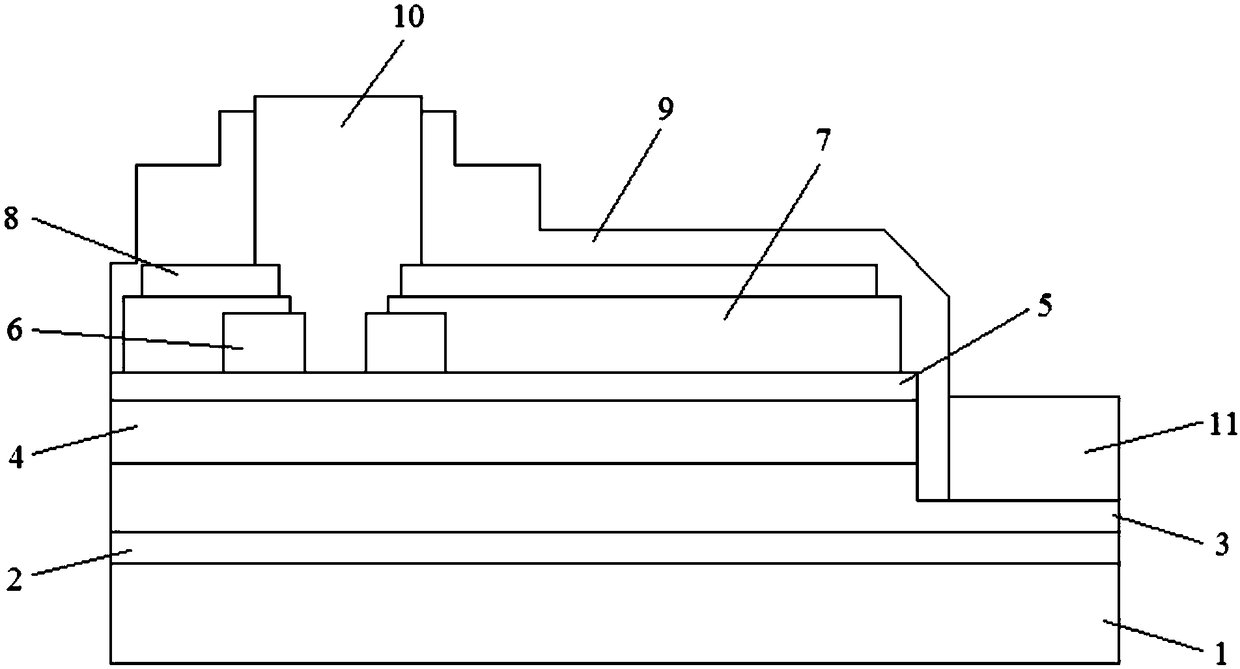
Figure 1 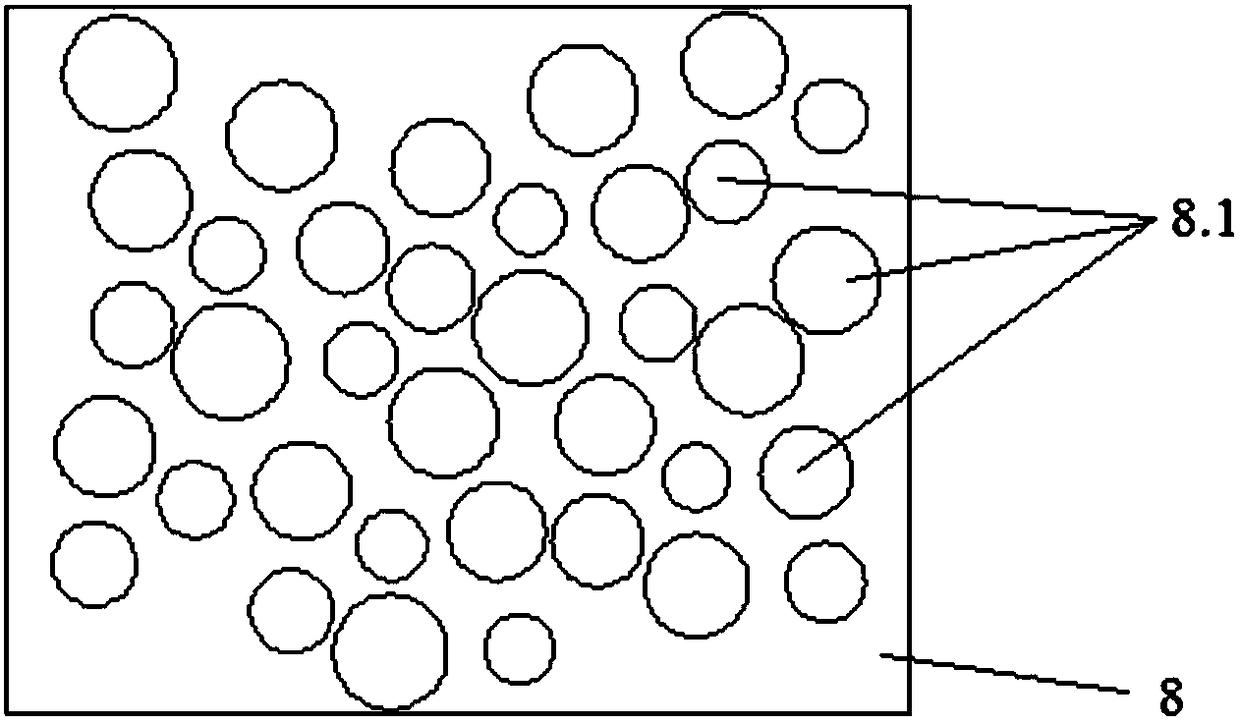
Figure 2
Abstract
Description
technical field
[0001] The invention relates to the technical field of semiconductor LEDs, in particular to an LED chip and a manufacturing method thereof. Background technique
[0002] At present, the third-generation semiconductor materials have been widely used in various fields of human production and life, and play an important role in them. Gallium nitride (GaN) material, as an important part of the third-generation semiconductor material family, has also been widely used, and it plays an irreplaceable role in the LED semiconductor industry. GaN material is a hexagonal wurtzite structure, which has the advantages of stable chemical properties, high temperature resistance, large band gap, and high electron drift saturation velocity. Therefore, GaN-based materials are widely used in the preparation of electronic devices such as LED chips, blue LEDs, green LEDs, and ultraviolet LEDs, and are widely used in various fields of production and life such as lighting, medical t...
Examples
Embodiment 1
[0045] In order to better describe the present invention, an embodiment of the present invention provides a method for manufacturing a high-brightness LED, including the following steps:
[0046] 1. On the sapphire substrate 1, a buffer layer 2, an N-type GaN layer 3, a multi-quantum well layer 4, and a P-type GaN layer 5 are sequentially grown on the sapphire substrate 1 by MOCVD, thereby preparing an LED epitaxial wafer ; Wherein, the thickness of the epitaxial layer of the LED epitaxial wafer is 6.5 μm.
[0047] 2. Deposit a layer of SiO on the epitaxial wafer by PECVD 2 film, with a thickness of The pattern (CB pattern) of the current blocking layer is prepared by photolithography etching, and the photoresist is removed to obtain the current blocking layer 6; the current blocking layer is provided with a P-region electrode hole for subsequent formation of a P-type electrode.
[0048] 3. Evaporate a layer of indium tin oxide film (ITO) on the LED epitaxial wafer by sputt...
Embodiment 2
[0055] The embodiment of the present invention provides another method for manufacturing a high-brightness LED chip, including the following steps:
[0056] 1. On the sapphire substrate 1, a buffer layer 2, an N-type GaN layer 3, a multi-quantum well layer 4, and a P-type GaN layer 5 are sequentially grown on the sapphire substrate 1 by MOCVD, thereby preparing an LED epitaxial wafer ; Wherein, the thickness of the epitaxial layer of the LED epitaxial wafer is 6.5 μm.
[0057] 2. Deposit a layer of SiO on the epitaxial wafer by PECVD 2 film, SiO 2 The thickness of the film is The pattern (CB pattern) of the current blocking layer is etched and prepared by photolithography, and the photoresist is removed to obtain the current blocking layer 6 .
[0058] 3. A layer of indium tin oxide thin film (ITO) is vapor-deposited on the epitaxial wafer by sputtering, and as the current spreading layer 7, the thickness of the indium tin oxide thin film is And evaporate a layer of simpl...