
Tunable broadband low-noise amplifier
A broadband low-noise, amplifier technology, applied in the field of radio frequency, can solve the problems of deteriorating receiver sensitivity, out-of-band signal interference, and high cost, and achieve the effects of being conducive to miniaturized design, achieving gain flatness, and improving power
Patent Information
- Authority / Receiving Office
- CN · China
- Patent Type
- Applications(China)
- Current Assignee / Owner
- Publication Date
- 2020-01-21
Smart Images
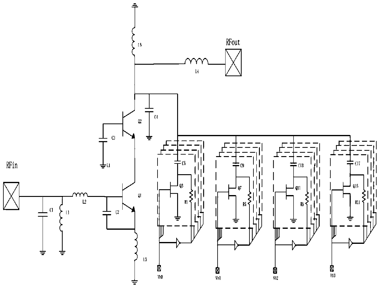
Figure 1 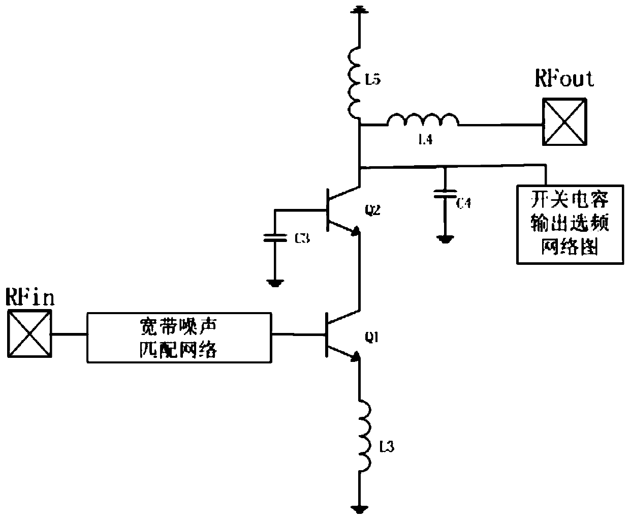
Figure 2 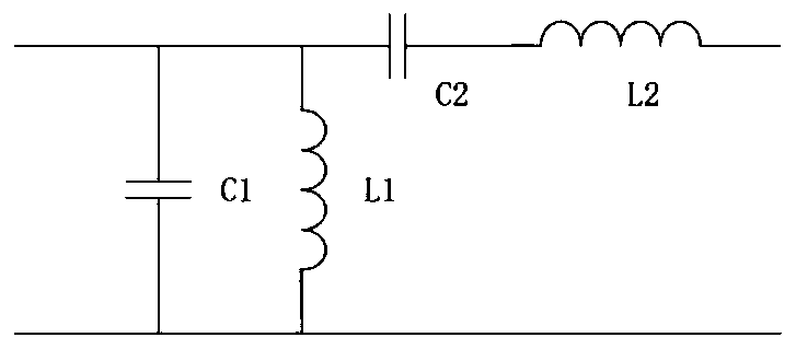
Figure 3
Abstract
Description
technical field
[0001] The invention relates to the field of radio frequency technology, in particular to a tuneable broadband low noise amplifier. Background technique
[0002] With the rapid development of wireless communication technology, a series of wireless communication protocols have been formulated internationally. In order to meet various needs, multi-frequency and multi-mode mobile terminals have become a new direction of wireless communication development. On the other hand, the rapid popularization of portable devices has stricter requirements on the miniaturization and low power consumption of the devices, and the miniaturization and low power consumption of wireless communication radio frequency modules are more urgent. As an important device for wireless communication, the low noise amplifier needs to process the signal received by the antenna and reduce the noise of the communication module. Therefore, the low noise amplifier is very important for the whol...
Examples
Embodiment Construction
[0025] In order to clarify the purpose, technical solution and advantages of the present invention more clearly, the present invention will be further described below in conjunction with the accompanying drawings.
[0026] Such as figure 2 , the tunable broadband low-noise amplifier is composed of a broadband noise matching network, a switched capacitor output frequency selection network and a common-source common-gate amplifier circuit structure; the amplifier circuit is a cascode (common-source common-gate) structure, which uses a common-source transistor , the first transistor Q1 and the second transistor Q2, the drain of the first transistor Q1 is connected to the source of the second transistor Q2, and the overall circuit performance is optimized by using the source inductance negative feedback, wherein the third inductance L3 is the source negative feedback inductance, connected The source of the first transistor Q1 can improve the stability of the circuit and provide t...