
Cascaded distributed low-noise amplifier
A technology of low-noise amplifiers and amplifiers, applied in amplifiers, radio frequency amplifiers, amplifier types, etc., can solve problems such as the inability to effectively increase the gain-bandwidth product of amplifiers, and achieve the effects of simple structure, excellent radio frequency indicators, and low input return loss
Patent Information
- Authority / Receiving Office
- CN · China
- Patent Type
- Applications(China)
- Current Assignee / Owner
- Publication Date
- 2018-07-27
Smart Images
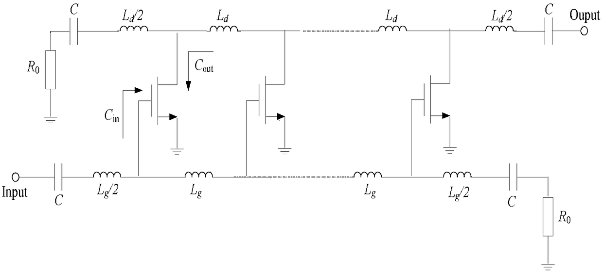
Figure 1 
Figure 2 
Figure 3
Abstract
Description
technical field
[0001] The invention relates to a cascaded distributed low noise amplifier, which belongs to the technical field of radio frequency integrated circuits. Background technique
[0002] The rapid development of wireless communication technology puts forward higher requirements on the data transmission rate and bandwidth of the communication system. Commonly used broadband amplifier design techniques include negative feedback, balanced amplifiers, resistor matching, and active matching, etc., but none of these techniques can effectively improve the gain-bandwidth product of the amplifier. Due to its structural characteristics, the distributed amplifier can break through the limitation of the gain-bandwidth product of the amplifier and realize wider-band signal amplification.
[0003] Monolithic microwave integrated circuits are widely used in many fields such as wireless communication, satellite communication network, millimeter wave automatic collision avoidanc...
Examples
Embodiment Construction
[0018] Embodiments of the present invention will be described below in conjunction with the accompanying drawings.
[0019] The basic principle of the traditional distributed low noise amplifier is to form an artificial transmission line with the parasitic capacitance of the transistor and the inductance element, so as to overcome the gain roll-off caused by the parasitic capacitance. The circuit schematic diagram is as follows figure 1 Shown, where vdd is the supply voltage, vgs is the DC bias voltage, the on-chip inductor Lg and the input impedance of the gain unit constitute the input artificial transmission line, and the on-chip inductor Ld and the output impedance of the gain unit constitute the output artificial transmission line. Obviously, the input / output artificial transmission lines are all low-pass filter structures.
[0020] According to the principle analysis of the distributed low noise amplifier, the input and output terminals of the distributed low noise ampl...