
Inductor-free low-noise amplifier with separated gain and impedance matching
A low-noise amplifier and impedance matching technology, which is applied to amplifiers, improved amplifiers to improve efficiency, and amplifier input/output impedance improvements. It can solve the problems of mutual limitation between impedance matching and amplification gain, and achieve improved flexibility and easy system gain. , the effect of large system gain
Patent Information
- Authority / Receiving Office
- CN · China
- Current Assignee / Owner
- Publication Date
- 2020-04-03
Smart Images
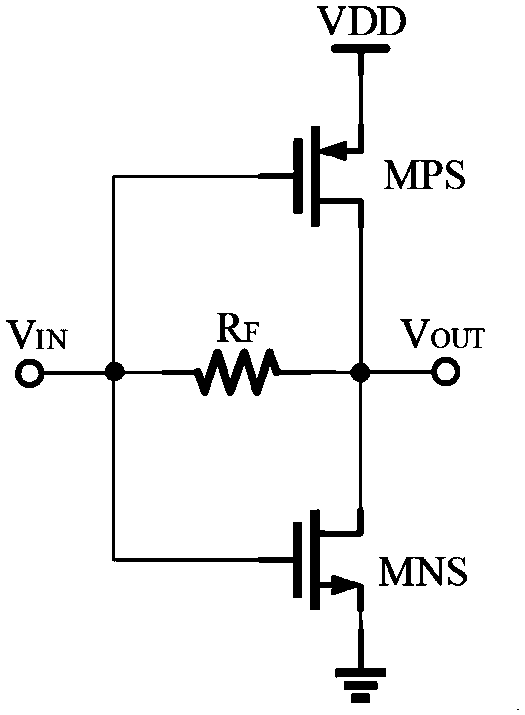
Figure 1 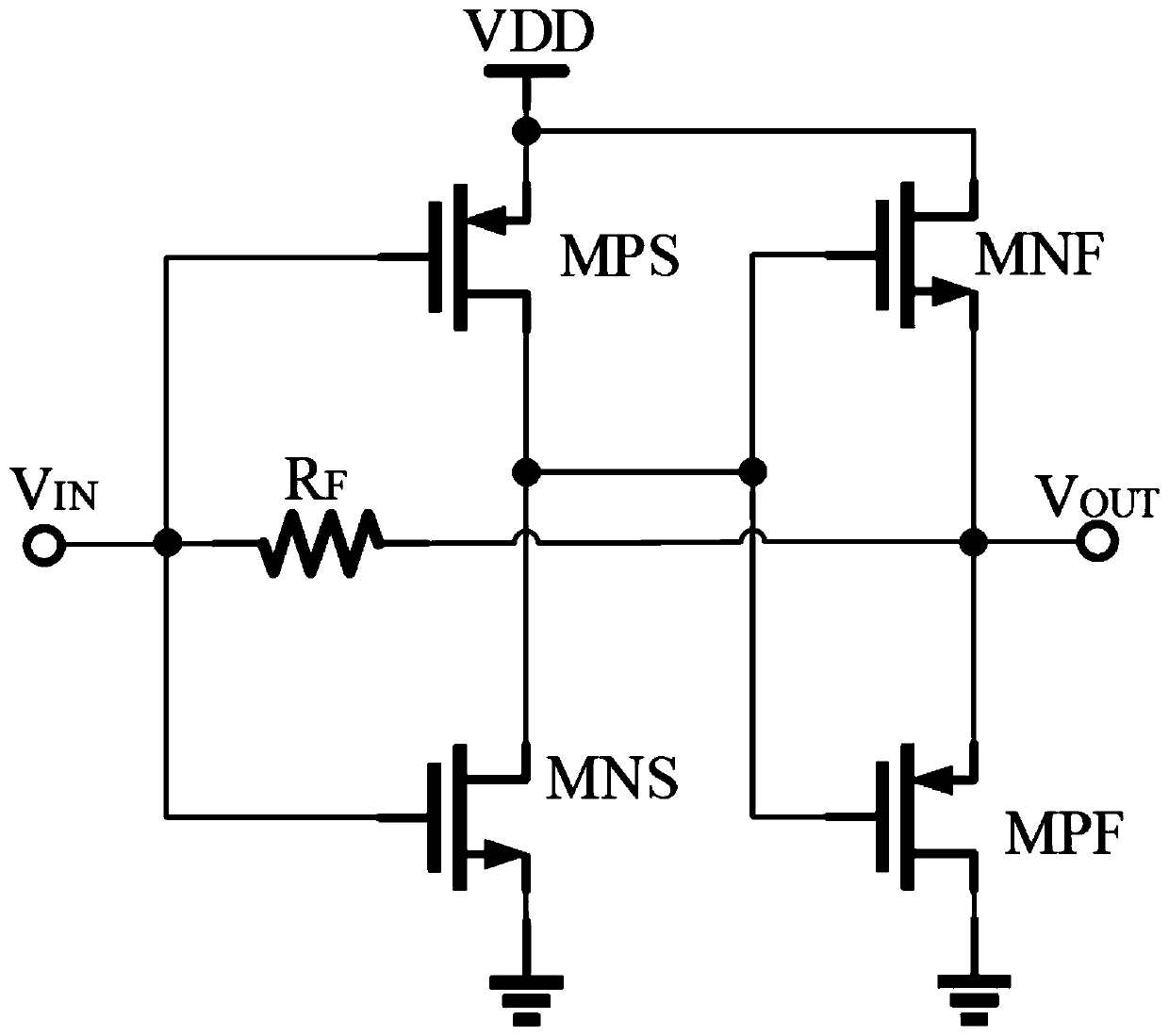
Figure 2 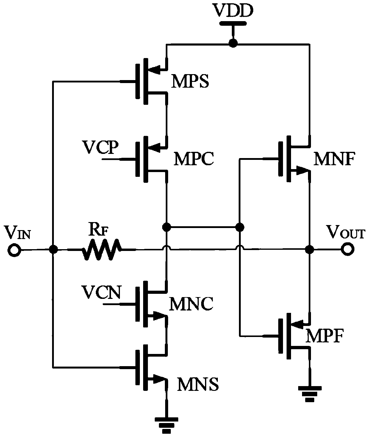
Figure 3
Abstract
Description
technical field
[0001] The invention relates to the technical field of radio frequency integrated circuits, in particular to a non-inductive low-noise amplifier with separated gain and impedance matching. Background technique
[0002] With the increasing application of the Internet of Things, the demand for wireless communication chips is becoming more and more urgent. In the front end of the RF transceiver, the general non-inductive low noise amplifier (Low Noise Amplifier, LNA) adopts a common source amplifier circuit with resistive feedback, and uses a feedback resistor to feed back a current from the output voltage to the input terminal.
[0003] In order to achieve low-noise amplification, the LNA needs to consider the input impedance matching and amplification gain; the traditional non-inductor LNA uses a common-source amplifier circuit with resistive feedback, and the feedback resistor needs to meet both impedance matching and amplification gain; the RF receiving fron...
Examples
Embodiment 1
[0042] As the first stage of the RF receiver, the low noise amplifier receives and amplifies the RF signal from the RF antenna, in order to reduce the R F simultaneous effects on gain and input impedance, this embodiment provides as figure 2 The shown two-stage circuit structure combines resistive feedback with a voltage buffer (voltage buffer) circuit, and the voltage buffer adopts a source follower circuit structure.
[0043] Such as figure 2 The circuit structure shown consists of three parts:
[0044]1. The first-stage amplifying circuit composed of a push-pull amplifier;
[0045] 2. Voltage buffer level composed of source follower;
[0046] 3. Feedback resistor R F .
[0047] The working process of this embodiment is:
[0048] The signal from the antenna of the RF receiver passes through the impedance matching network to the input terminal V of the first stage amplifier circuit IN , the first stage is used as the main gain stage, the second stage provides the vol...
Embodiment 2
[0069] Such as image 3 As shown, on the basis of Embodiment 1, the first-stage push-pull amplifier in Embodiment 2 adopts a cascode circuit structure, and the circuit performance is better improved when the circuit principle remains unchanged. .
[0070] VCN and VCP are DC bias voltages of MOS tubes MNC and MPC respectively, and MNC and MNS, MPC and MPS respectively form a cascode structure.