
Preparation of SiC MOSFET based on high-k gate dielectric and low-temperature ohmic contact process
A technology of ohmic contact and gate dielectric, applied in semiconductor/solid-state device manufacturing, electrical components, transistors, etc., can solve problems such as low mobility, achieve the effect of reducing carbon cluster density and improving channel mobility
Patent Information
- Authority / Receiving Office
- CN · China
- Current Assignee / Owner
- Publication Date
- 2020-10-02
- Estimated Expiration
- Not applicable · inactive patent
Smart Images
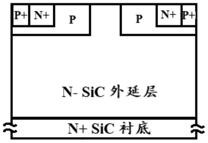
Figure 1 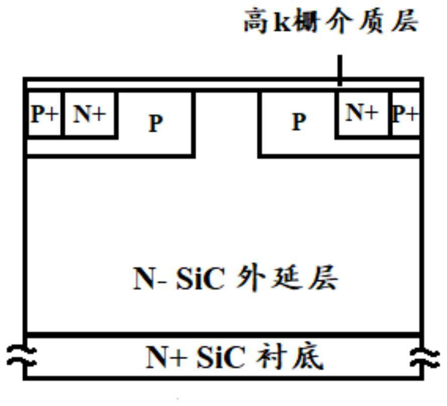
Figure 2 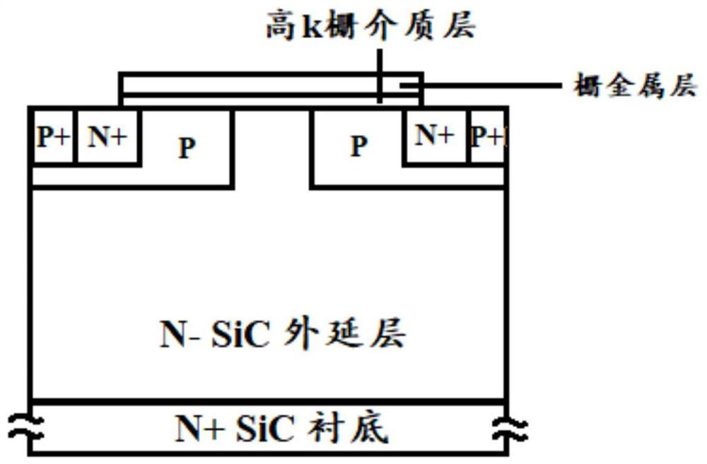
Figure 3
Abstract
Description
technical field
[0001] The invention belongs to the field of semiconductor power devices, in particular to a method for preparing a SiC MOSFET based on a high-k gate dielectric and a low-temperature ohmic contact process. Background technique
[0002] Silicon carbide material has a large band gap, high breakdown electric field, large thermal conductivity and stable physical properties, and is an excellent high-power, high-voltage, high-temperature power semiconductor device manufacturing material. Since silicon carbide has N and P types through doping, and natural oxidation to generate SiO 2 The characteristics, so its preparation process is highly compatible and similar to the traditional silicon power device process, and a relatively mature process has been developed on this basis.
[0003] Metal Oxide Semiconductor Field Effect Transistor (MOSFET) is a widely used electronic device. It is a majority carrier device, which avoids minority carrier injection when bipolar tr...
Examples
Embodiment 1
[0042] (1) The epitaxial N-type lightly doped SiC layer (thickness 13 μm, doping concentration 6×10 13 cm -3 ) SiC substrate cleaning; the cleaning process includes: standard RCA cleaning; high-temperature oxidation of silicon carbide epitaxial wafers to form a sacrificial oxide layer, and then corrode the sacrificial oxide layer until the surface oxide layer is completely removed.
[0043] (2) if figure 1 As shown, three kinds of implanted regions can be formed in the substrate. The three injection regions are respectively a P-type injection region, an N+ type injection region, and a P+ type injection region. Specifically, the N+ type implantation region is arranged between the P and P+ type implantation regions. P-type and P+-type implantation regions are formed by implanting aluminum and phosphorus ions. According to the embodiment, can inject 10 15 -10 18 cm -3 Doping concentration of P-type ions. Similarly, an N+ type implantation region is formed by implanting n...
Embodiment 2
[0054] The high-k dielectric layer in step (3) in Example 1 can be replaced. In this example, the ALD method is used to grow La 2 o 5 (5nm) / Al 2 o 3 (45nm) medium layer, its thickness can be selected as 50nm. Other conditions do not change, and are all identical with embodiment 1.
[0055] Calculation process is identical with embodiment 1, for this laminated structure C ox =5.5×10 -11 F / m, other experimental data remain unchanged. In this embodiment, the interface state density can reach 7×10 11 -10 12 cm -2 eV -1 , with a mobility of 35cm 2 / Vs, the critical breakdown electric field strength can reach 8.7MV / cm.
Embodiment 3
[0057] The high-k dielectric layer in step (3) in Example 1 can be replaced. In this example, SiO grown by CVD method is selected. 2 (5nm) / AlN(45nm) dielectric layer, the thickness of which can be 50nm. Other conditions do not change, and are all identical with embodiment 1.
[0058] Calculation process is identical with embodiment 1, for this laminated structure C ox =6.2×10 -11 F / m, other experimental data remain unchanged. In this embodiment, the interface state density can reach 7×10 10 -4×10 12 cm -2 eV -1 , with a mobility of 26cm 2 / Vs, the critical breakdown electric field can reach 16.8MV / cm.