

Semiconductor device
Patent Information
- Authority / Receiving Office
- US · United States
- Current Assignee / Owner
- Publication Date
- 2007-02-22
- Estimated Expiration
- Not applicable · inactive patent
Smart Images
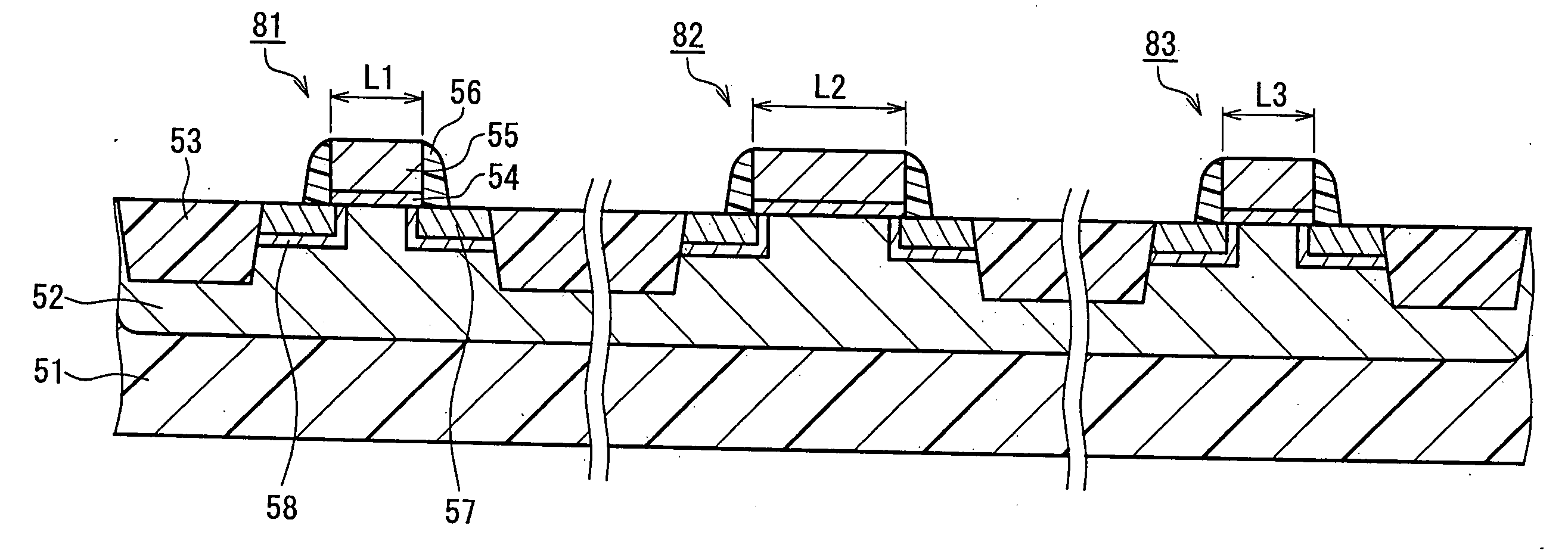
Figure 1 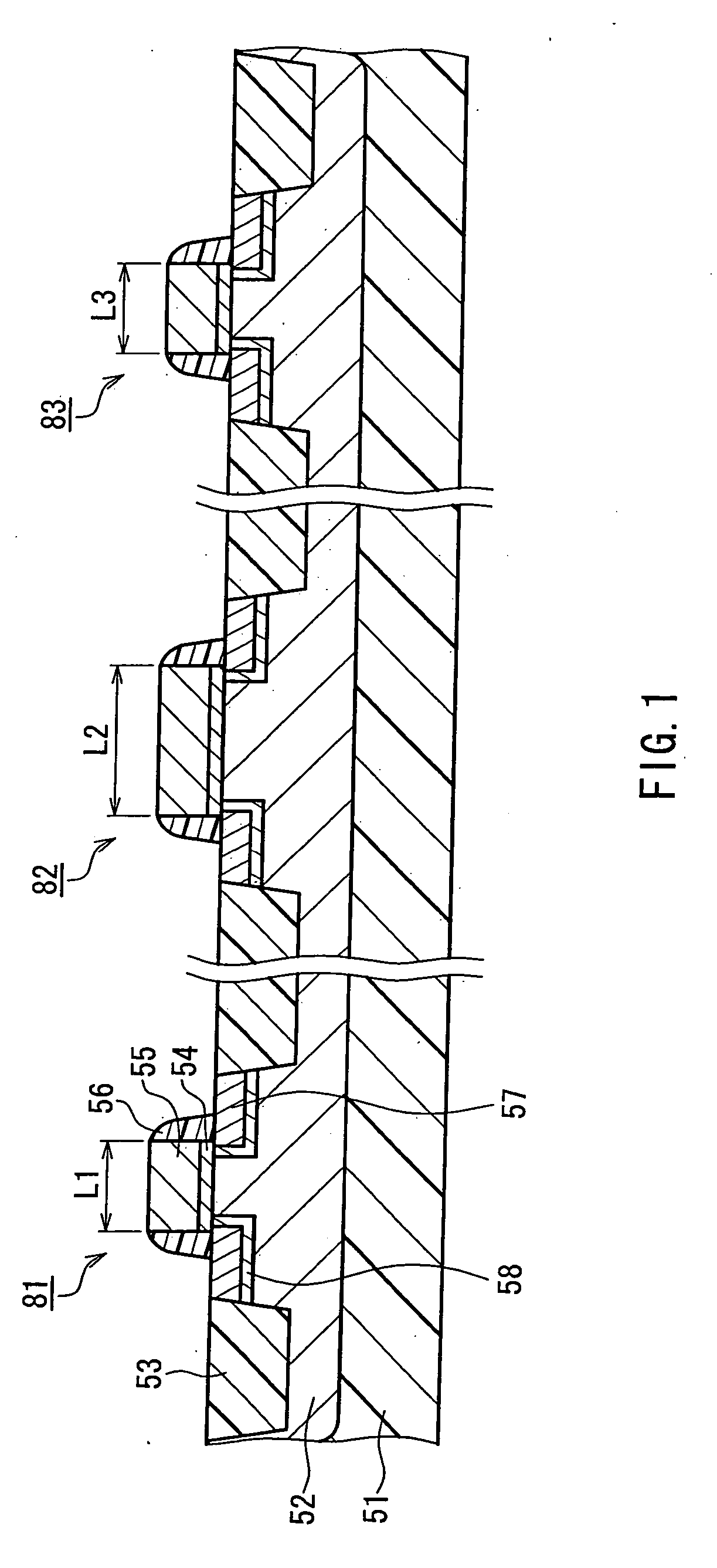
Figure 2 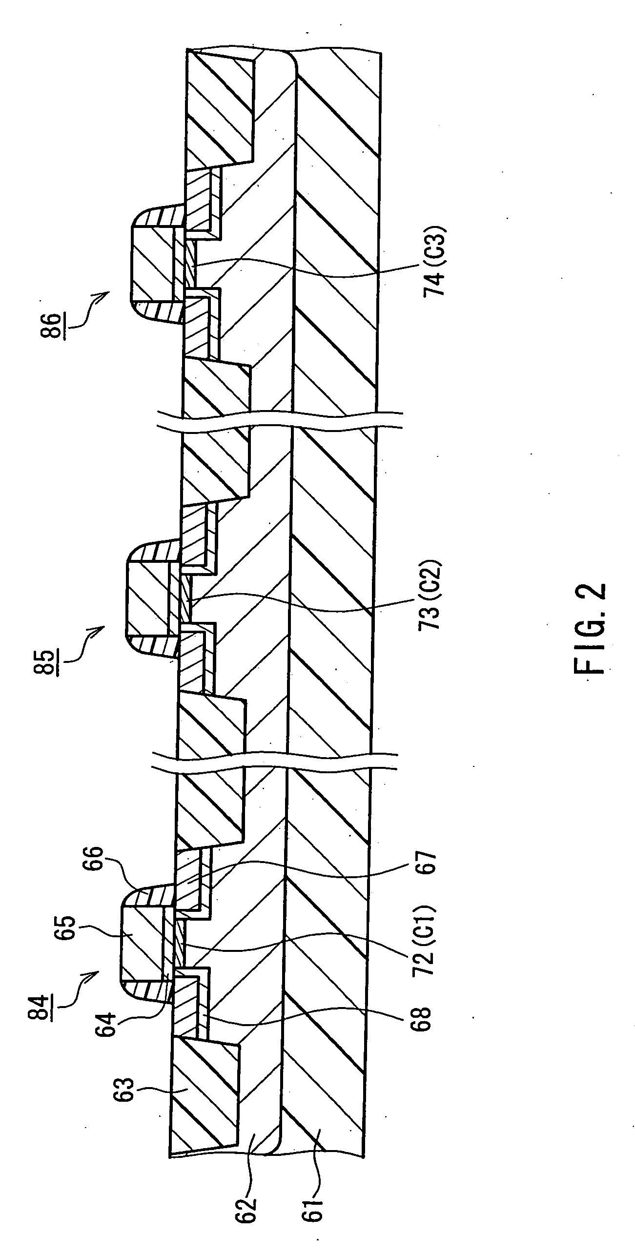
Figure 3
Abstract
Description
BACKGROUND OF THE INVENTION
[0001] 1. Field of the Invention
[0002] The present invention relates to a semiconductor device that can be used effectively in a solid-state imaging device including: a photosensitive region in which a plurality of photosensitive cells are disposed in a matrix; a driving circuit for driving the plurality of photosensitive cells that is constituted by a dynamic circuit; a scanning circuit for selecting the plurality of photosensitive cells; and a bootstrap circuit for transmitting a selection signal from the scanning circuit to a driving circuit. In particular, the present invention relates to the bootstrap circuit.
[0003] 2. Description of Related Art
[0004] In recent years, attention has been directed to a solid-state imaging apparatus provided with an amplification-type MOS sensor, as one of solid-state imaging apparatuses. In this solid-state imaging apparatus, a signal detected by a photodiode is amplified by a transistor for each cell (pixel), and t...
Examples
embodiment 1
[0044]FIG. 1 is a cross-sectional view of a semiconductor device of Embodiment 1. In FIG. 1, only a selection transistor 81, a booster transistor 82 and a peripheral logic transistor 83 that are provided in the semiconductor device are described.
[0045] The semiconductor device of the present embodiment is used in an MOS type solid-state imaging apparatus that is manufactured by a miniaturized CMOS logic technology with a size of 0.25 μm or less, in which element isolation is performed by STI (Shallow Trench Isolation), and a gate oxide film is formed to have a film thickness of 10 nm or less.
[0046] As shown in FIG. 1, each of the selection transistor 81, the booster transistor 82 and the peripheral logic transistor 83 includes: a p-well 52; an element isolation region 53 (hereinafter, called STI) that electrically isolates each of the transistor elements; a gate oxide film 54 that is formed above the p-well 52; a gate electrode 55 that is formed above the gate oxide film 54; a sid...
embodiment 2
[0058]FIG. 2 is a cross-sectional view of a semiconductor device of Embodiment 2. In FIG. 2, only a selection transistor 84, a booster transistor 85 and a peripheral logic transistor 86 that are provided in the semiconductor device are described.
[0059] The semiconductor device of Embodiment 2 is an MOS type solid-state imaging apparatus that is manufactured by a miniaturized CMOS logic technology with a size of 0.25 μm or less, in which element isolation is performed by STI, and a gate oxide film is formed to have a film thickness of 10 nm or less.
[0060] As shown in FIG. 2, each of the selection transistor 84, the booster transistor 85 and the peripheral logic transistor 86 includes: a p-well 62; an element isolation region 63 (hereinafter, called STI) that electrically isolates each of the transistor elements; a gate oxide film 64 that is formed above the p-well 62; a gate electrode 65 that is formed above the gate oxide film 64; a side wall 66 that protects sides of the gate oxi...