
Nitride semiconductor laser device and wafer
a laser device and semiconductor technology, applied in semiconductor lasers, semiconductor/solid-state device details, optical beam sources, etc., can solve the problems of increasing cost and productivity, impractical for actual mass production, and reducing efficiency, so as to increase the noise reduction effect of high-frequency superposition circuit, reduce capacitance, and improve response
Patent Information
- Authority / Receiving Office
- US · United States
- Patent Type
- Applications(United States)
- Current Assignee / Owner
- Publication Date
- 2010-12-30
Smart Images
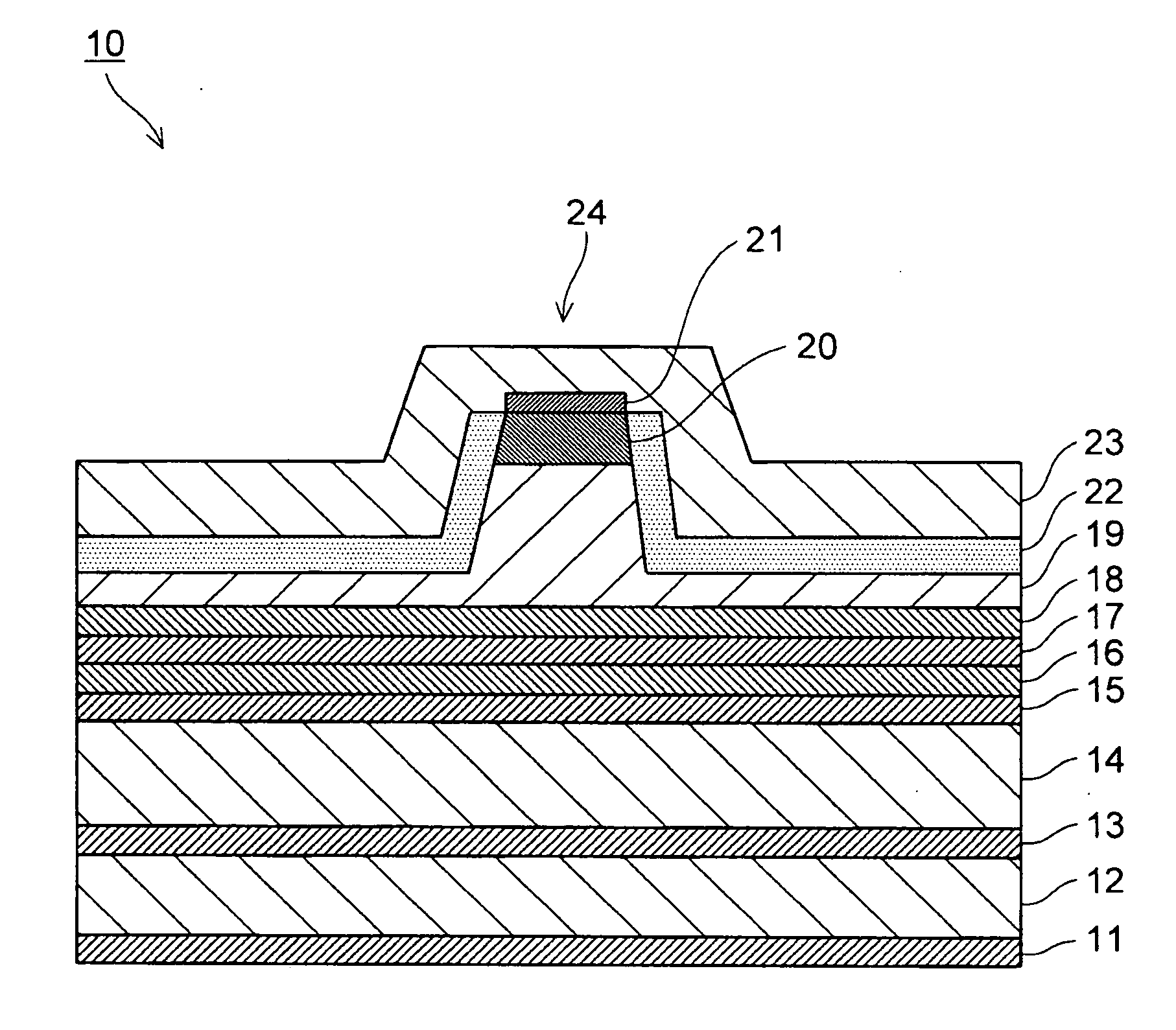
Figure 1 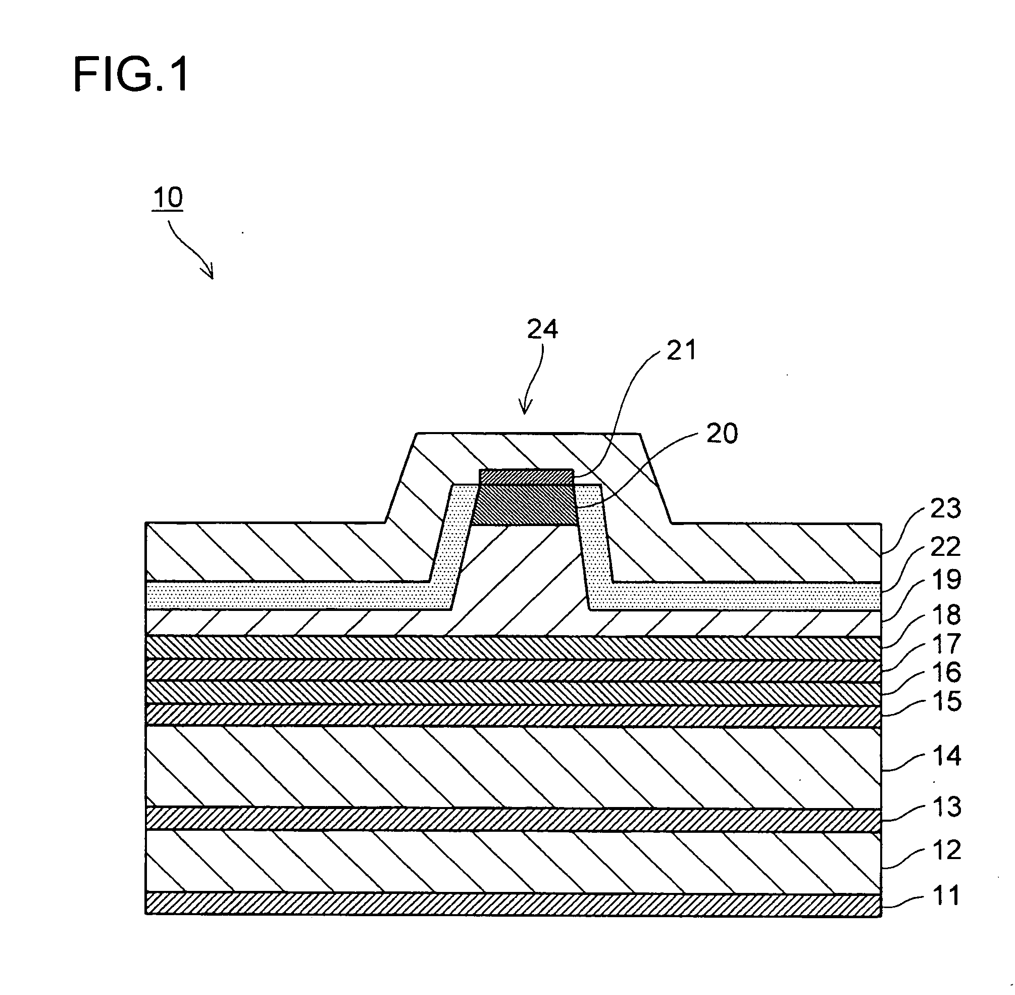
Figure 2 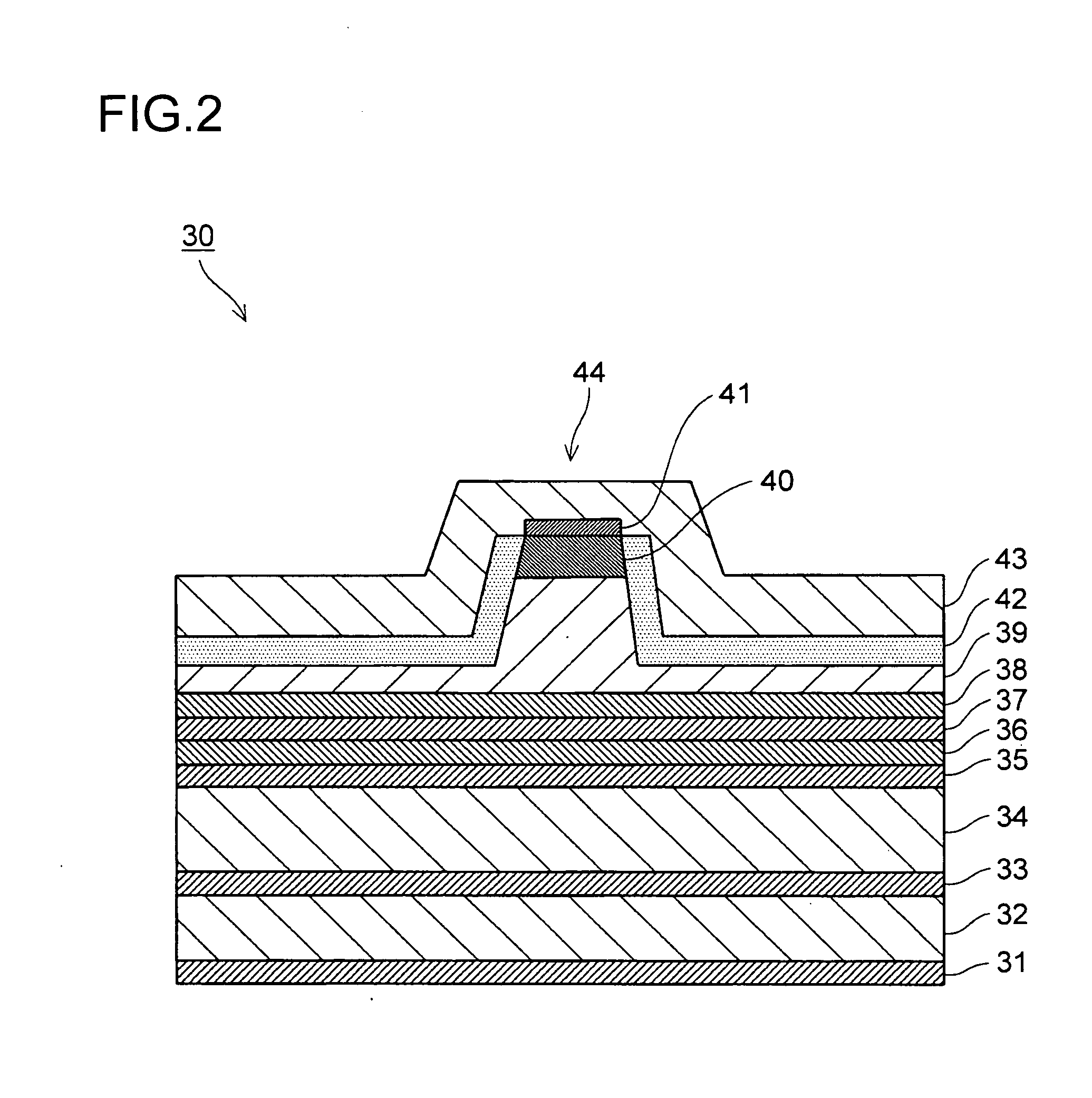
Figure 3
Abstract
Description
[0001] The present application claims priority from Japanese Patent Application No. 2009-153470 filed on Jun. 29, 2009, the content of which is hereby incorporated by reference into this application.BACKGROUND OF THE INVENTION
[0002] 1. Field of the Invention
[0003] The present invention relates to a wafer in which a plurality of nitride semiconductor laser devices to be separated from one another are arranged, and to a nitride semiconductor laser device obtained from the wafer.
[0004] 2. Description of Related Art
[0005] Nitride semiconductor laser devices, which are utilized in the recording and playing of a Blu-ray disc or the like and other uses, are being actively researched and developed. For example, to record information at a high density, turning laser light on and off fast is required and a laser device is accordingly driven with short pulses of approximately 20 ns. In pulsed operation, where a laser device exhibits a better response when its impedance is smaller, reducing the resi...
Examples
first embodiment
[0041]FIG. 1 is a sectional view of a nitride semiconductor laser device according to a first embodiment. The nitride semiconductor laser device denoted by 10 is built by stacking an n-type electrode 11, an n-type GaN substrate 12, an n-type GaN buffer layer 13, an n-type AlGaN cladding layer 14, an n-type GaN / InGaN light guiding layer 15, a non-doped GaN / InGaN active layer 16, a p-type AlGaN vaporization preventing layer 17, a p-type GaN or AlGaN interlayer 18, a p-type AlGaN cladding layer 19, a p-type GaN contact layer 20, a Pd contact electrode 21, a low dielectric constant insulating film 22, and a Ti / Au pad electrode 23.
[0042]The nitride semiconductor laser device 10 is manufactured by first growing, on the n-type GaN substrate 12, by metal organic chemical vapor deposition (hereinafter abbreviated as MOCVD), the n-type GaN buffer layer 13, the n-type AlGaN cladding layer 14, the n-type GaN / InGaN light guiding layer 15, the non-doped GaN / InGaN active layer 16, the p-type AlGaN...
second embodiment
[0048]FIG. 2 is a sectional view of a nitride semiconductor laser device according to a second embodiment. The nitride semiconductor laser device denoted by 30 is built by stacking an n-type electrode 31, an n-type GaN substrate 32, an n-type GaN buffer layer 33, an n-type AlGaN cladding layer 34, an n-type GaN / InGaN light guiding layer 35, a non-doped GaN / InGaN active layer 36, a p-type GaN or AlGaN interlayer 37, a p-type AlGaN vaporization preventing layer 38, a p-type AlGaN cladding layer 39, a p-type GaN contact layer 40, a Pd contact electrode 41, a high dielectric constant insulating film 42, and a Ti / Au pad electrode 43.
[0049]The nitride semiconductor laser device 30 is manufactured by first growing, on the n-type GaN substrate 32, by metal organic chemical vapor deposition (hereinafter abbreviated as MOCVD), the n-type GaN buffer layer 33, the n-type AlGaN cladding layer 34, the n-type GaN / InGaN light guiding layer 35, the non-doped GaN / InGaN active layer 36, the p-type GaN...
third embodiment
[0055]A third embodiment of the present invention uses a processed substrate that is an n-type GaN substrate with grooves formed in a stripe pattern in its top face (epitaxy face). The processed substrate is manufactured by first forming an SiO2 film or the like on the top face of an n-type GaN substrate by sputtering evaporation to a thickness of 1 μm, and forming a stripe photoresist pattern by a common lithography process such that the photoresist pattern has a width of 5 μm at a resist opening and an interval (cycle) of 400 μm between the center of a stripe and the center of an adjacent stripe.
[0056]Next, the SiO2 film and the n-type GaN substrate are etched by dry etching such as reactive ion etching (RIE) technology to form grooves each having a depth of 5 μm and an opening width of 5 μm. The SiO2 film is then removed with the use of an etchant such as HF, to thereby obtain the processed substrate.
[0057]The deposition by evaporation of SiO2 is not limited to sputtering evapora...