
Method and a structure for enhancing electrical insulation and dynamic performance of mis structures comprising vertical field plates
a vertical field plate and electrical insulation technology, applied in the field of semiconductor devices, can solve the problems of superior transistor characteristics, fuelled the development of complex integrated circuits, and extremely complex circuits
Patent Information
- Authority / Receiving Office
- US · United States
- Patent Type
- Applications(United States)
- Current Assignee / Owner
- Publication Date
- 2012-06-14
Smart Images
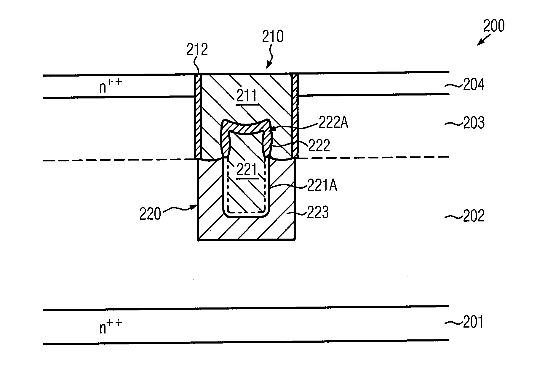
Figure 1 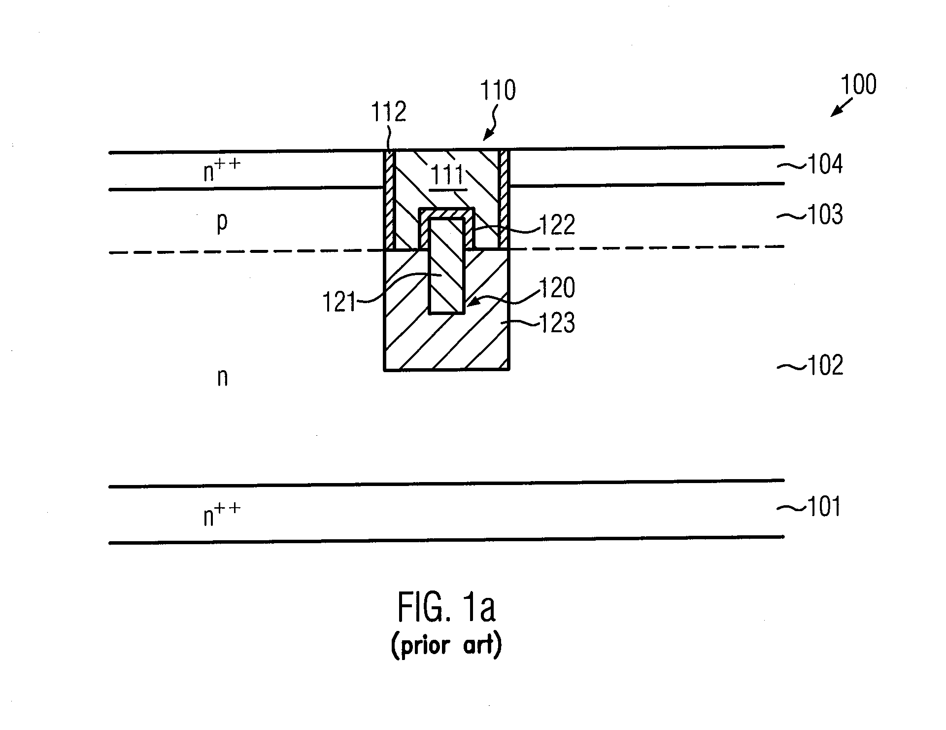
Figure 2 
Figure 3
Abstract
Description
BACKGROUND
[0001] 1. Technical Field
[0002] The present disclosure generally relates to semiconductor devices including MIS (metal-insulator-semiconductor) structures formed using a “vertical” device architecture in which a current flow may be controlled by electric field more efficiently on the basis a “buried” field plate.
[0003] 2. Description of the Related Art
[0004] In the field of semiconductor devices immense progress has been achieved by reducing the dimensions of the circuit elements and improving associated process techniques and process tools. The continuous shrinkage of critical feature sizes has, at one cutting edge of the semiconductor technology, resulted in the fabrication of extremely complex integrated circuits which may comprise millions of transistor elements, which may be operated using extremely low supply voltages. On the other hand, the advances in materials, process techniques and process tools have also fuelled the development of complex integrated circuits, which...
Examples
Embodiment Construction
[0036]In one aspect of the present disclosure, a method is provided that relates to forming an MIS structure wherein the method comprises forming a first semiconductor electrode in a cavity that is formed in a crystalline semiconductor region, wherein the first semiconductor electrode is electrically insulated from the crystalline semiconductor region by an insulating layer. The method further comprises increasing an oxidation rate of at least a portion of a surface of the first semiconductor electrode relative to an exposed surface of the crystalline semiconductor region in the cavity. Additionally, the method comprises concurrently oxidizing the exposed surface of the crystalline semiconductor region in the cavity and an exposed surface of the first semiconductor electrode so as to form a first oxide layer on the exposed surface of the crystalline semiconductor region and a second oxide layer on the exposed surface of the first semiconductor electrode. Finally, the method comprise...