
Capacitive force sensing touch panel
a capacitance force and touch panel technology, applied in the field of touch panel, can solve the problems of inaccurate force sensing results, force sensing determined according to capacitance variation, etc., and achieve the effect of avoiding noise interference of liquid crystal modules and being thinner and lighter
Patent Information
- Authority / Receiving Office
- US · United States
- Patent Type
- Applications(United States)
- Current Assignee / Owner
- Publication Date
- 2017-04-27
- Estimated Expiration
- Not applicable · inactive patent
Smart Images
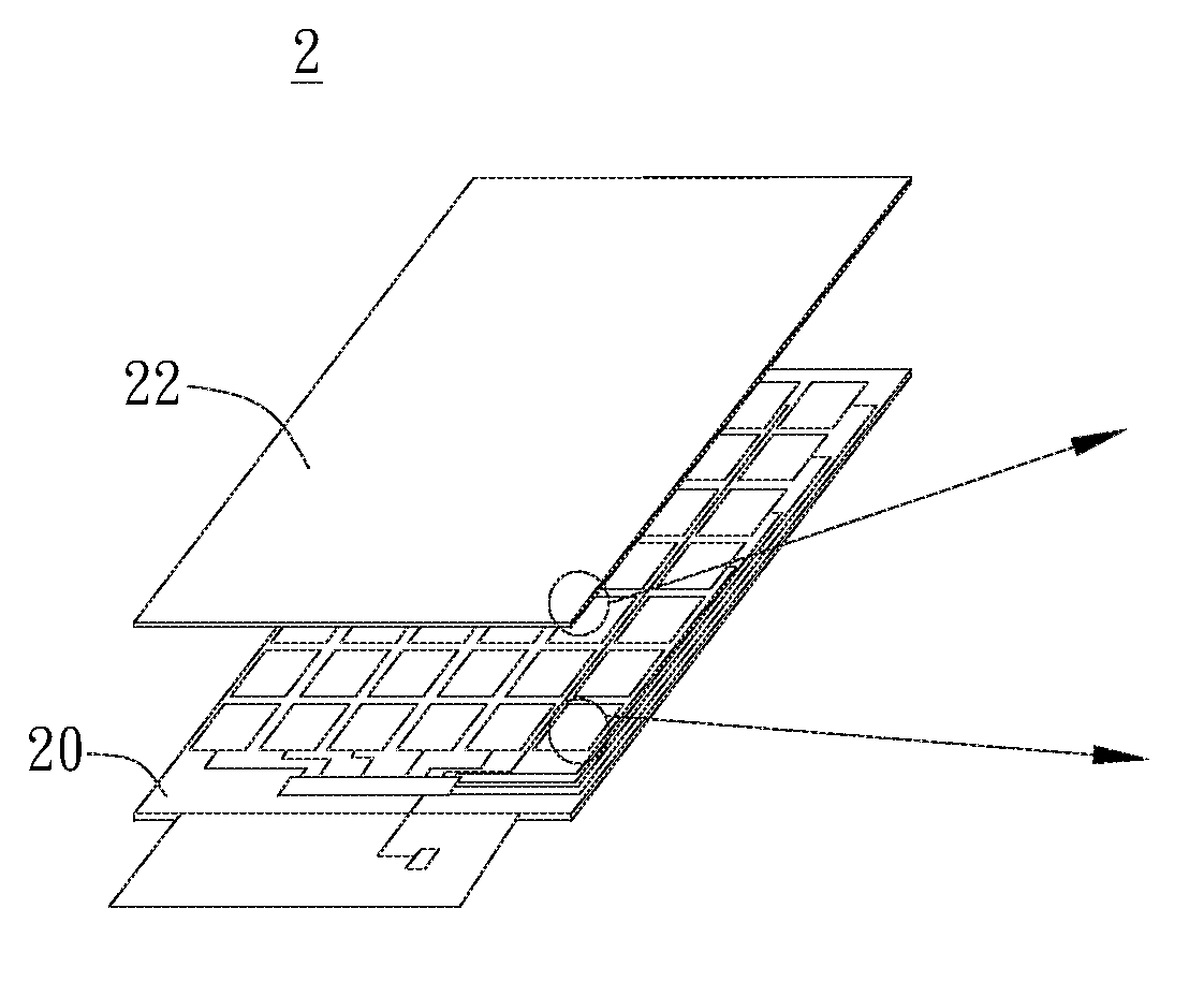
Figure 1 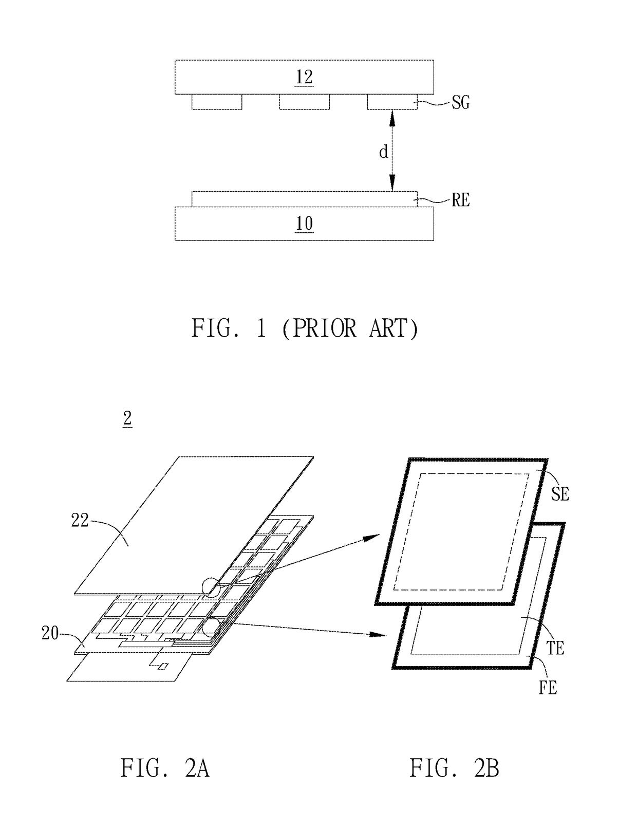
Figure 2 
Figure 3
Abstract
Description
BACKGROUND OF THE INVENTION
[0001] 1. Field of the Invention
[0002] This invention relates to touch panel, especially to a capacitive force sensing touch panel.
[0003] 2. Description of the Prior Art
[0004] In general, if capacitive touch electrodes in a capacitive touch panel are also used to be force sensing electrodes at the same time, such as the sensing electrode SG in FIG. 1 is disposed on the upper substrate 12. And, the reference electrode RE can be disposed on the lower substrate 10 in FIG. 1.
[0005] When the upper substrate 12 is pressed by a finger, because the distance d between the sensing electrode SE on the upper substrate 12 and the reference electrode RE on the lower substrate 10 will be changed based on different forces provided by the finger, the capacitance sensed between the sensing electrode SE and the reference electrode RE will be also changed accordingly.
[0006] However, the capacitive touch sensing signal will be also changed based on different finger pressing areas. W...
Examples
Embodiment Construction
[0063]The invention discloses a capacitive force sensing touch panel which can have an in-cell touch panel structure and use a relative upper shielding electrode to avoid the effects caused by the change of finger pressing area to maintain the accurate sensed capacitance during the force sensing period to improve the drawbacks of the prior arts.
[0064]At first, please refer to FIG. 2A and FIG. 2B. FIG. 2A and FIG. 2B illustrate schematic diagrams of the entire laminated structure and the unit electrode in the laminated structure of the node self-capacitive force sensing touch panel respectively in an embodiment of the invention.
[0065]As shown in FIG. 2A and FIG. 2B, the laminated structure 2 includes a first substrate 20 and a second substrate 22, and the second substrate 22 is disposed above the first substrate 20. In fact, the first substrate 20 and the second substrate 22 can be a TFT glass and a color filter glass respectively, but not limited to this.
[0066]In this embodiment, a ...