
Method for removal of residue from a magneto-resistive random access memory (MRAM) film stack using a sacrificial mask layer
Patent Information
- Authority / Receiving Office
- US · United States
- Current Assignee / Owner
- Publication Date
- 2006-01-10
- Estimated Expiration
- Not applicable · inactive patent
Smart Images
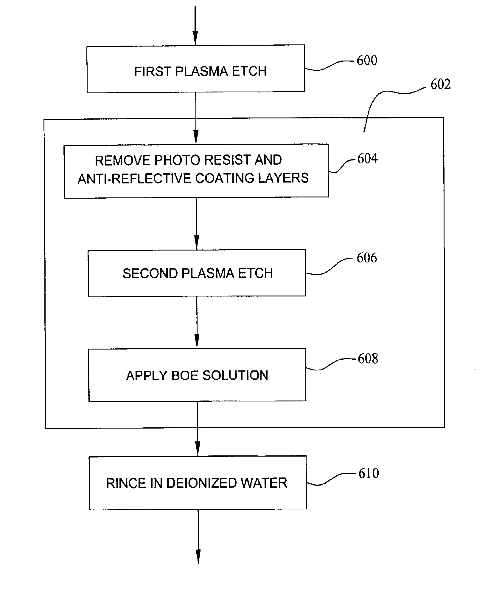
Figure 1 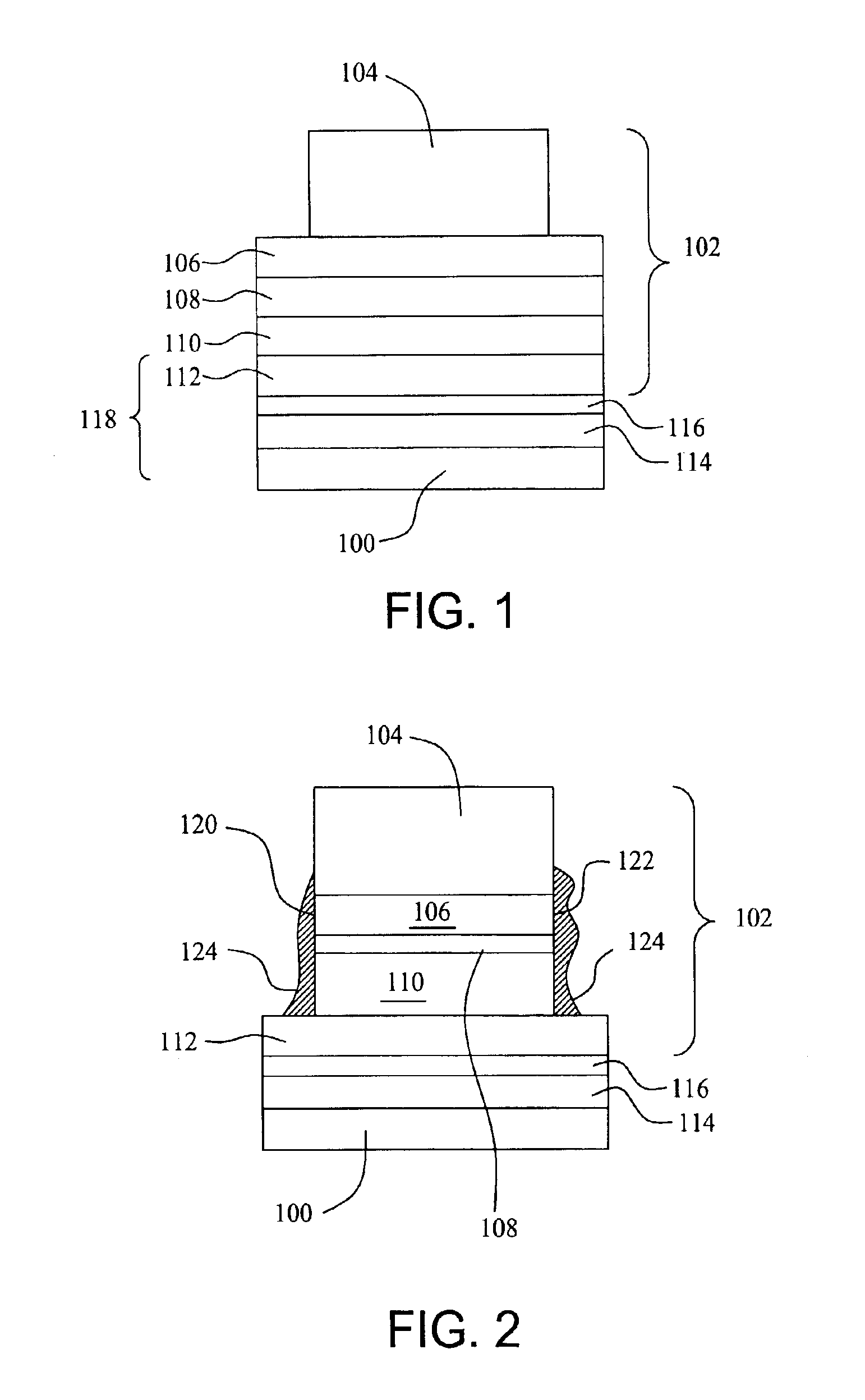
Figure 2 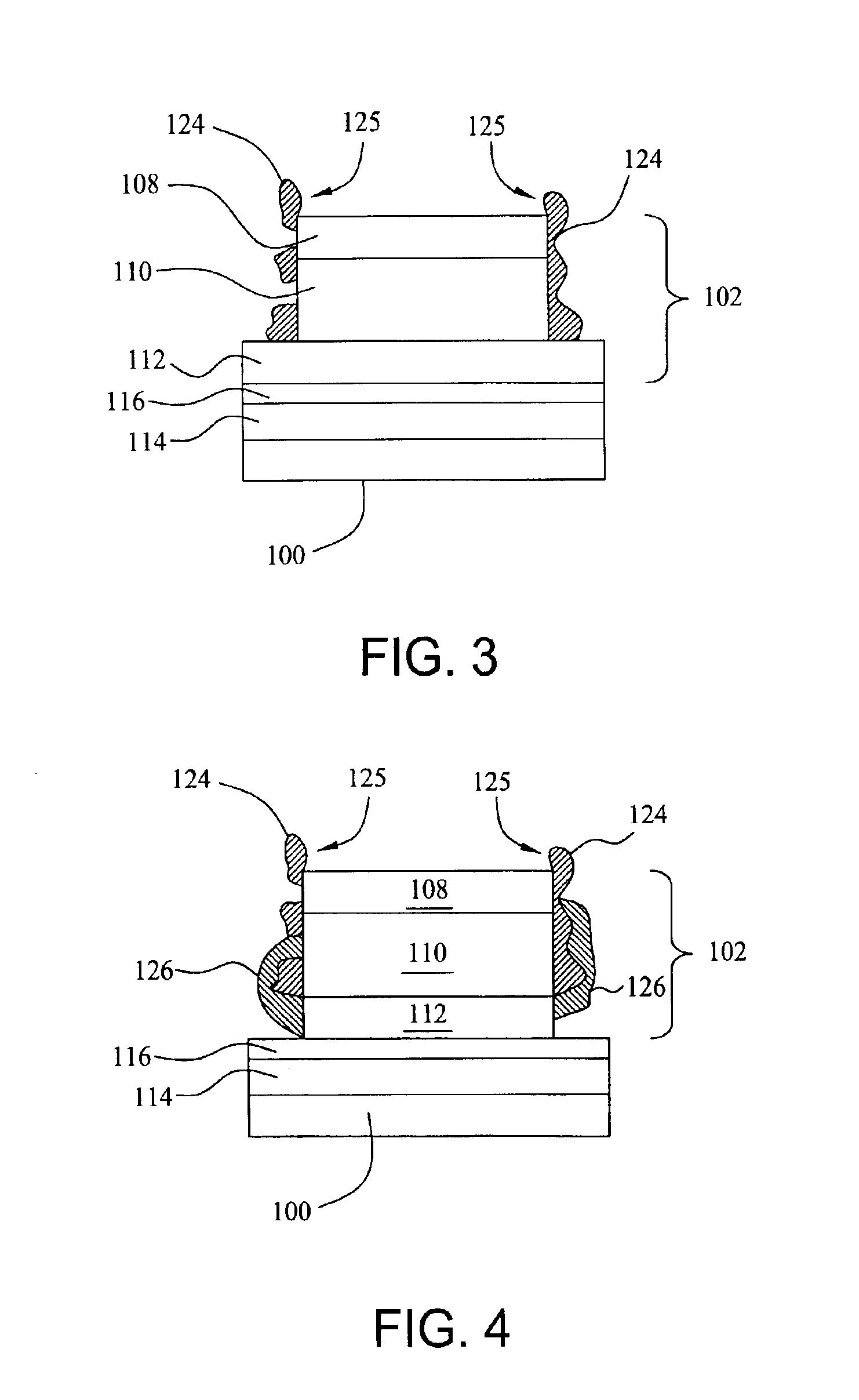
Figure 3
Abstract
Description
BACKGROUND OF THE INVENTION
[0001] 1. Field of the Invention
[0002] The present invention generally relates to a method for processing magneto-resistive random access memory (MRAM) film stacks. More specifically, the invention relates to a method for removal of residues after plasma etching a magneto-resistive random access memory (MRAM) film stack using a sacrificial silicon dioxide layer.
[0003] 2. Description of the Related Art
[0004] Microelectronic devices are generally fabricated on a semiconductor substrate as integrated circuits wherein various layers of metals must be interconnected to one another to facilitate propagation of electronic signals within the device. An example of such a device is the use of magnetic multilayer films, or film stacks, as a storage element in memories, such as magneto-resistive random access memories (MRAM). The magnetic multi-layer films are typically a stack of different layers composed of various materials, for example permalloy (NiFe), cobalt iron (C...
Examples
Embodiment Construction
[0021]The present invention is a method for removal of residues produced by plasma etching a magneto resistive random access memory (MRAM) film stack. The film stack contains a photoresist layer, an anti-reflective coating layer, a sacrificial layer, a conductive layer, a layer or layers of magnetic material and a tunneling layer. The sacrificial top layer, such as for example SiO2, is used as a hard mask for etching a layer or layers of magnetic material to the tunneling layer, such as for example alumina. Following a chlorine-based or fluorine based chemistry etching of the sacrificial top layer and conductive layer, a photoresist strip and an oxygen and chlorine-mixed chemistry etching for high selectivity to the tunneling layer, the residues, including the presence of any “veil”-like structures, as well as the sacrificial top layer, are removed using a buffered oxide etch (BOE) wet dip.
[0022]FIG. 1 is a schematic cross-sectional view of a substrate 100 before the photoresist str...