
Semiconductor system including a schottky diode
a schottky diode and semiconductor technology, applied in the direction of semiconductor devices, basic electric elements, electrical apparatus, etc., can solve the problems of high forward voltage uf, large dependence of reverse, and the schottky diode has not yet been used in the motor vehicle generator system. achieve the effect of flexible design capabilities, high degree of robustness, and achieve the degree of flexibility in designing components
Patent Information
- Authority / Receiving Office
- US · United States
- Patent Type
- Patents(United States)
- Current Assignee / Owner
- Publication Date
- 2014-09-16
Smart Images
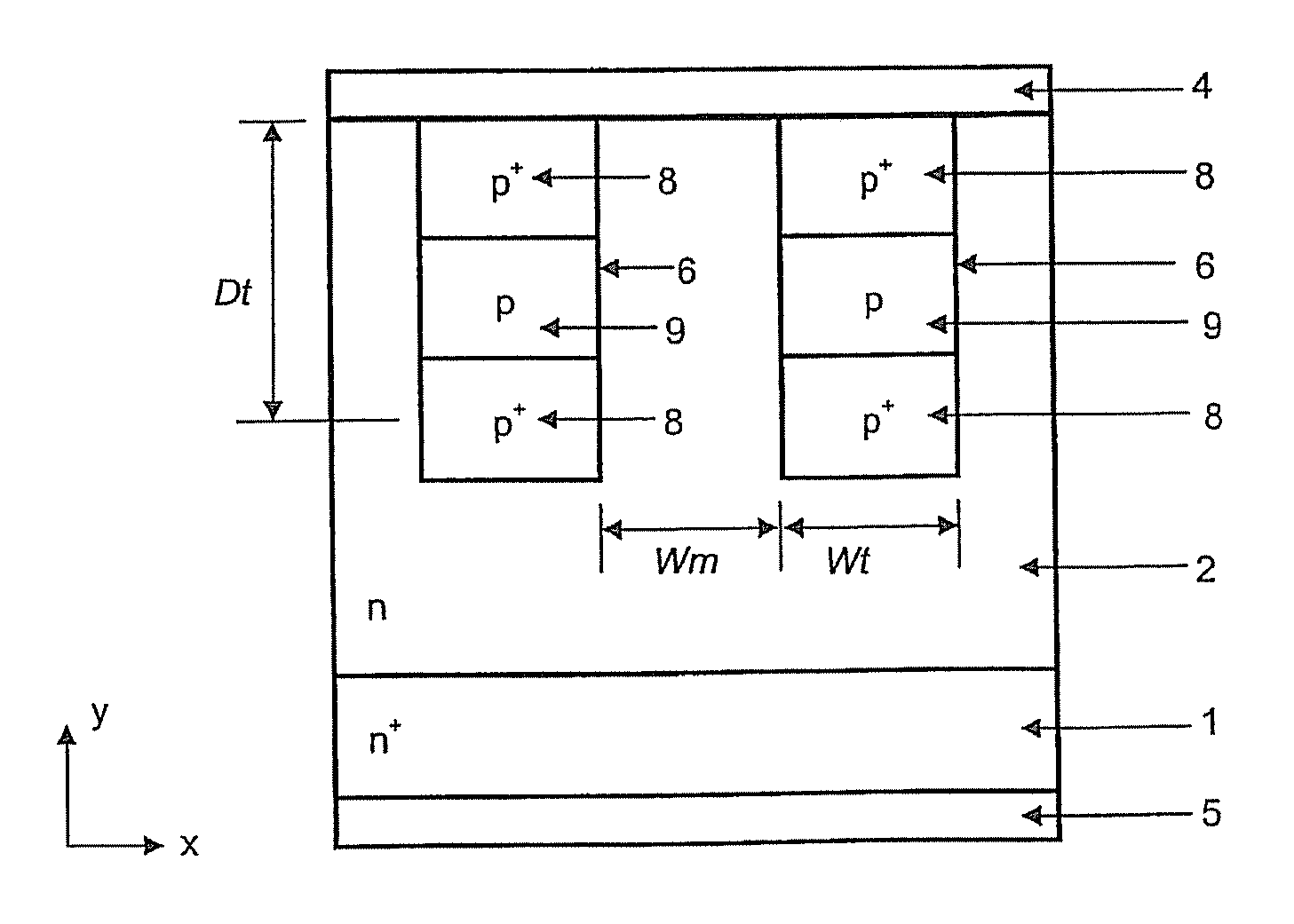
Figure 1 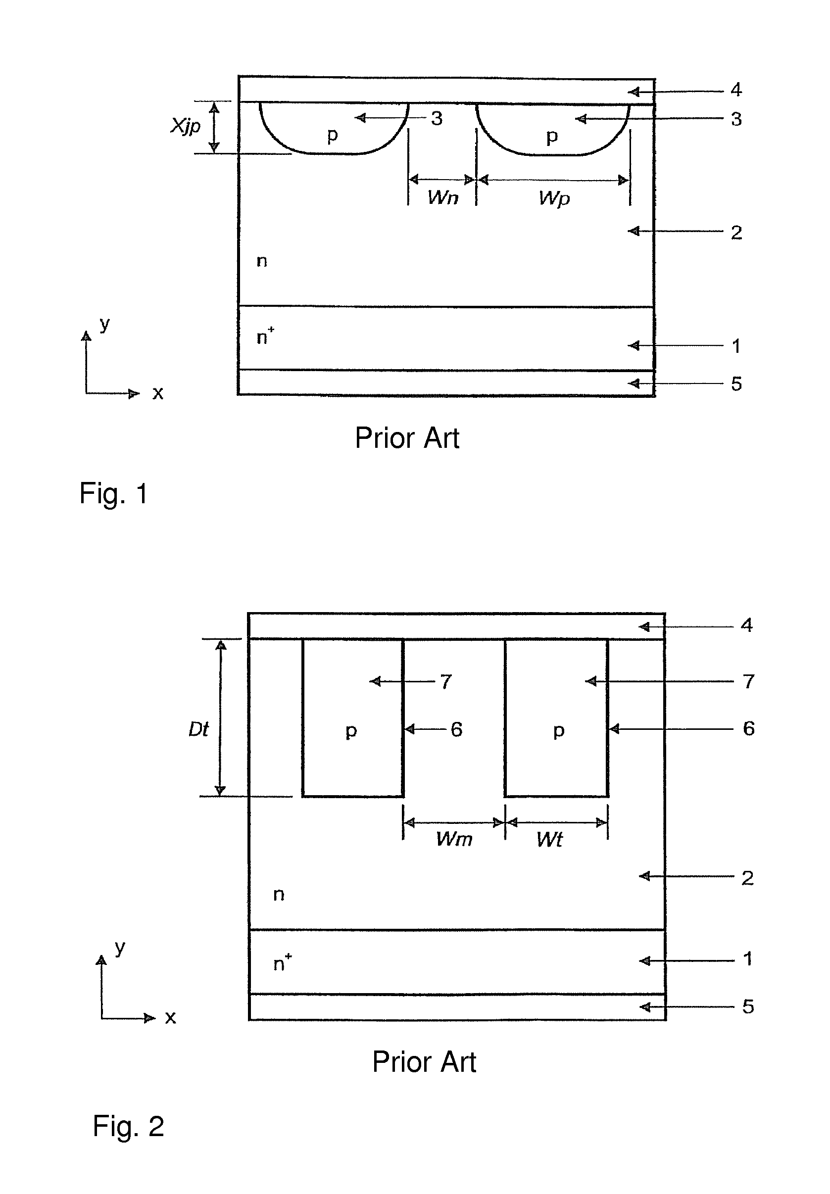
Figure 2 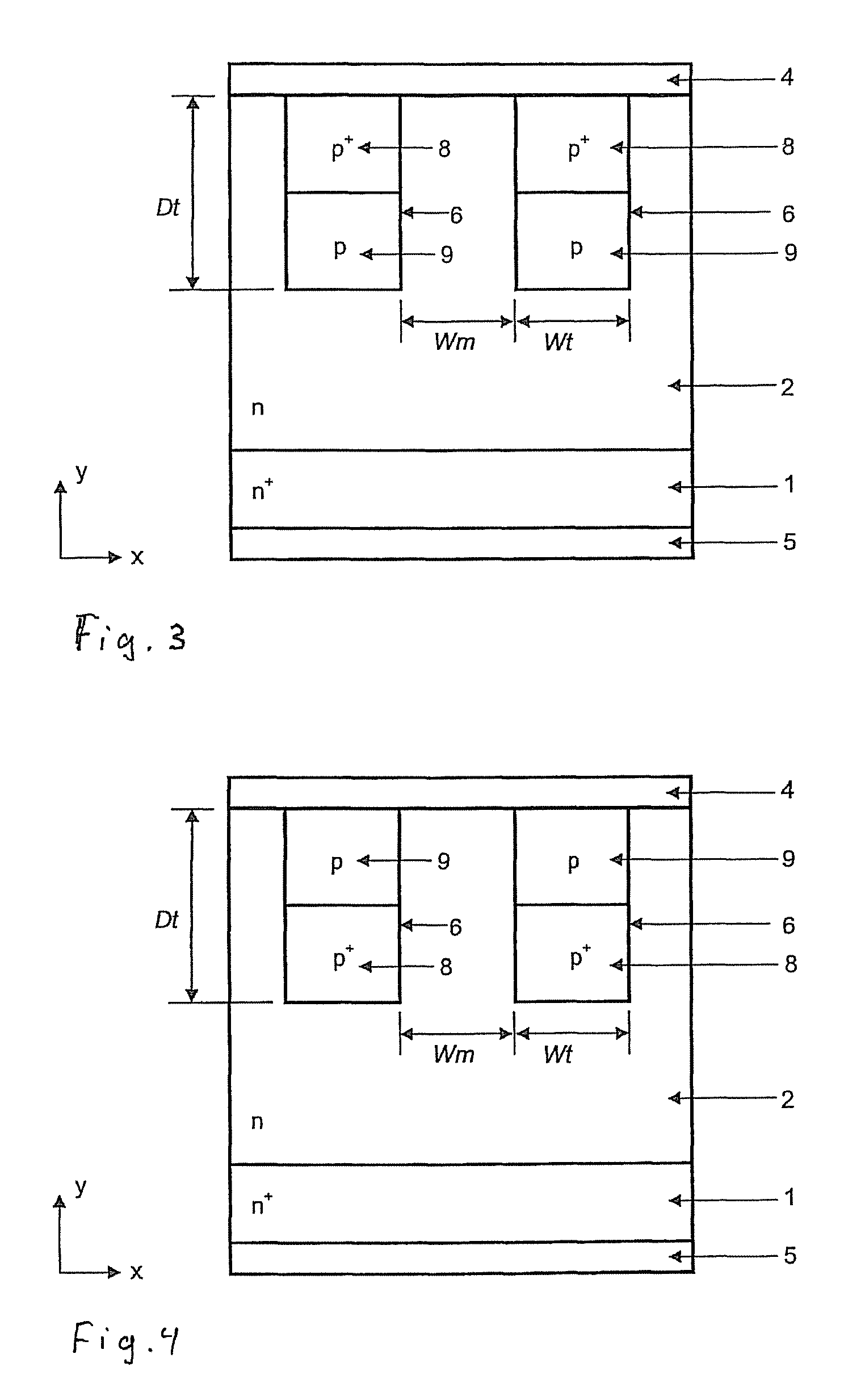
Figure 3
Abstract
Description
FIELD OF THE INVENTION
[0001] The present invention relates to variants of trench junction barrier Schottky diodes, which are referred below simply as TJBS.BACKGROUND INFORMATION
[0002] TJBS diodes offer greater flexibility for component design and are suitable, in particular, as Zener power diodes having a breakdown voltage of approximately 20V for use in motor vehicle generator systems.
[0003] More and more functions in modern motor vehicles are being performed by electrical components. This results in an ever higher demand for electrical power. To meet this demand, the efficiency of the generator system in the motor vehicle must be increased.
[0004] Until now, p-n type diodes have ordinarily been used as Zener diodes in motor vehicle generator systems. The advantages of p-n type diodes are a low reverse current, on the one hand, and high robustness, on the other hand. The main disadvantage is a high forward voltage UF. At room temperature, current begins to flow only at UF=0.7V. Under no...
Examples
exemplary embodiment 3
[0029]Additional exemplary embodiments of the present invention are illustrated in FIG. 5 and FIG. 6. In exemplary embodiment 3 in FIG. 5, the p-type well is divided into three areas from top to bottom; the middle area is filled with highly doped p+ Si or p+ poly-Si 8, and the upper and lower areas are filled with low-doped p Si or p poly-Si 9.
exemplary embodiment 4
[0030]In exemplary embodiment 4 in FIG. 6, the p-type well is also divided into three areas from top to bottom. The middle area is filled with low-doped p Si or p poly-Si 9, and the upper and lower areas are filled with highly doped p+ Si or p+ poly-Si 8. Compared to the TJBS variants illustrated in FIGS. 3 and 4, the two exemplary embodiments provide even greater flexibility in designing components, while minimizing additional process control complexity. In the TJBS variants of the present invention, currents flow only through the Schottky diode in the forward direction, as in a conventional JBS or TJBS, if the forward voltage of the TJBS variant according to the present invention is substantially lower than the forward voltage of the p-n type diode.
[0031]The TJBS variants according to the present invention provide a high degree of robustness due to the clamping function, as in the case of a TJBS illustrated in FIG. 2. The breakdown voltage of p-n type diode BV_pn is designed in su...