
Process for producing photovoltaic device and photovoltaic device
Patent Information
- Authority / Receiving Office
- US · United States
- Current Assignee / Owner
- Publication Date
- 2011-12-15
- Estimated Expiration
- Not applicable · inactive patent
Smart Images
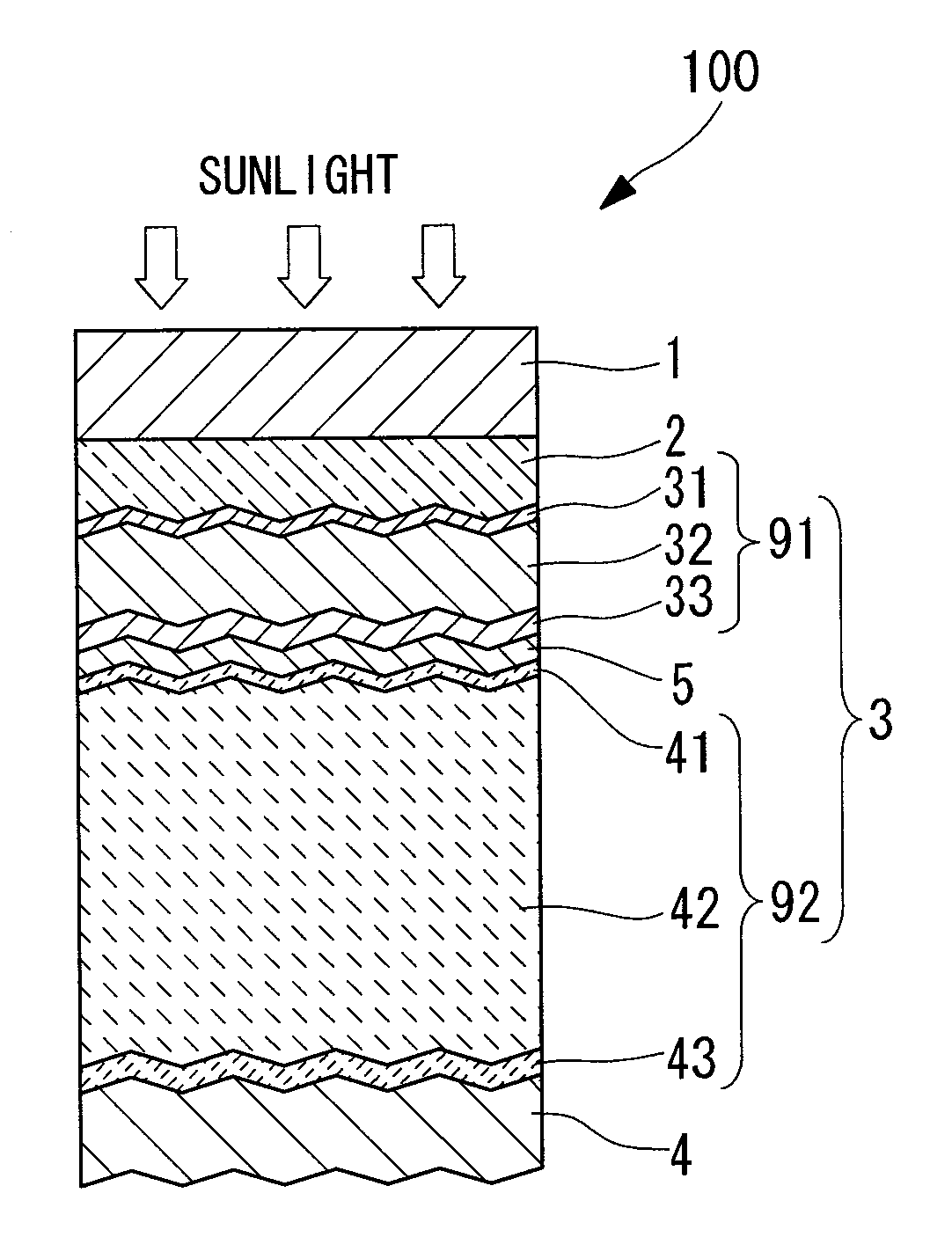
Figure 1 
Figure 2 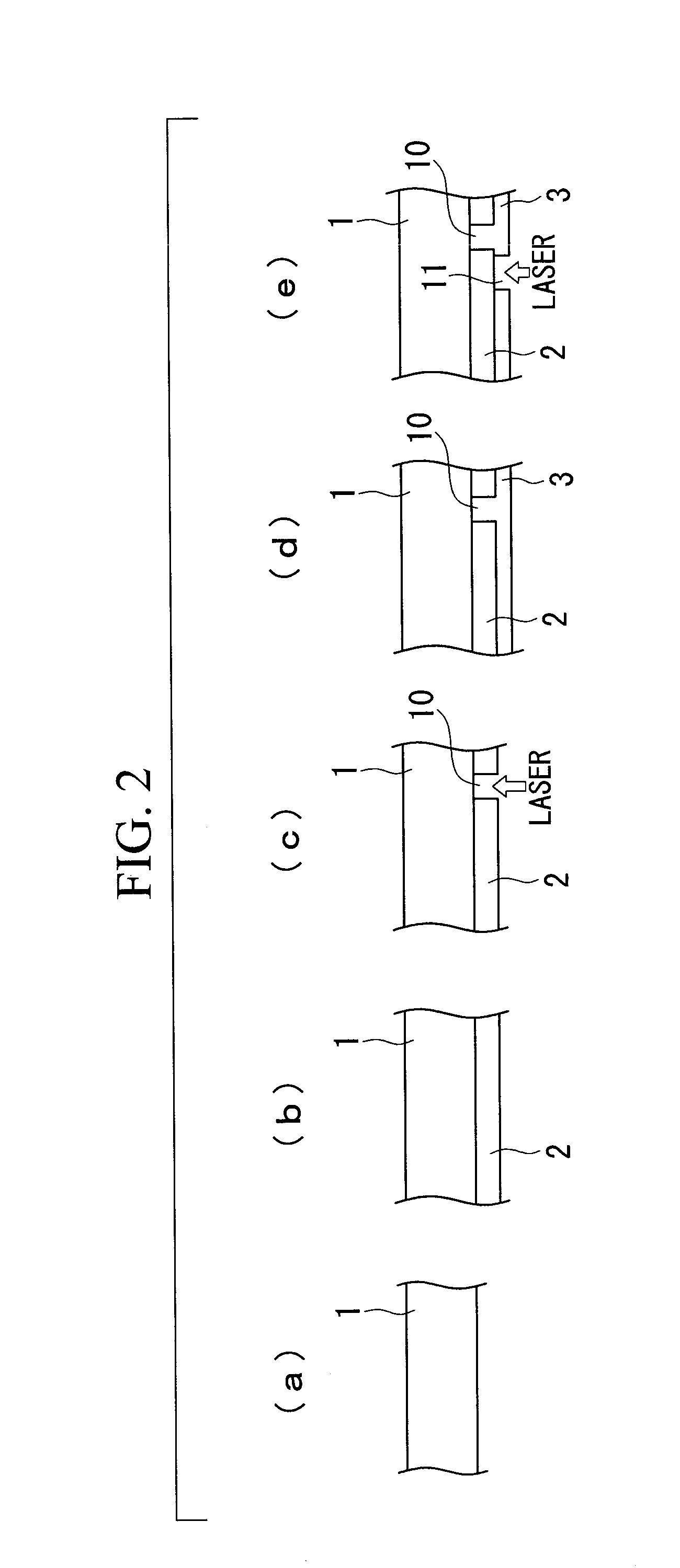
Figure 3
Abstract
Description
TECHNICAL FIELD
[0001] The present invention relates to a photovoltaic device, and relates particularly to a process for producing a thin-film silicon-based solar cell in which the electric power generation layer is formed by deposition, and a photovoltaic device prepared using this production process.BACKGROUND ART
[0002] One known example of a photovoltaic device that converts the energy from sunlight into electrical energy is a thin-film silicon-based solar cell comprising a photovoltaic layer formed by using a plasma enhanced CVD method or the like to deposit thin films of a p-type silicon-based semiconductor (p-layer), an i-type silicon-based semiconductor (i-layer) and an n-type silicon-based semiconductor (n-layer). Advantages of thin-film silicon-based solar cells include the comparative ease with which the surface area can be increased, and the fact that the film thickness is approximately 1 / 100th that of a crystalline solar cell, meaning minimal material is required. As a re...
Examples
Embodiment Construction
[0058]FIG. 1 is a schematic representation illustrating the structure of a photovoltaic device according to the present invention. A photovoltaic device 100 is a tandem silicon-based solar cell, and comprises a substrate 1, a transparent electrode layer 2, a first cell layer 91 (amorphous silicon-based) and a second cell layer 92 (crystalline silicon-based) as a photovoltaic layer 3, an intermediate contact layer 5, and a back electrode layer 4. Here, the term “silicon-based” is a generic term that includes silicon (Si), silicon carbide (SiC) and silicon germanium (SiGe). Further, the term “crystalline silicon-based” describes a silicon system other than an amorphous silicon system, and includes both microcrystalline silicon systems and polycrystalline silicon systems.
[0059]An embodiment in which the production process according to the present invention is applied to the deposition of a crystalline silicon i-layer is described below, using the production steps for a solar cell panel...