A Comparative Research on Resistive RAM and Other Memory Techs
OCT 9, 20259 MIN READ
Generate Your Research Report Instantly with AI Agent
Patsnap Eureka helps you evaluate technical feasibility & market potential.
ReRAM Technology Background and Objectives
Resistive Random Access Memory (ReRAM) has emerged as a promising non-volatile memory technology in the evolving landscape of semiconductor memory solutions. The concept of resistive switching was first observed in the 1960s, but significant research momentum only began in the early 2000s when limitations of conventional memory technologies became increasingly apparent. ReRAM's development trajectory has been driven by the growing demand for faster, more energy-efficient, and higher-density memory solutions capable of supporting next-generation computing paradigms.
The fundamental operating principle of ReRAM relies on the reversible change in resistance of a dielectric material, typically a metal oxide, under applied electrical stress. This resistance switching mechanism enables binary data storage, with high and low resistance states representing "0" and "1" respectively. Unlike charge-based memories, ReRAM stores information through physical changes in material structure, offering inherent non-volatility and potential for multi-bit storage.
The evolution of ReRAM technology has been characterized by continuous improvements in switching materials, electrode configurations, and fabrication processes. Early implementations faced challenges with reliability, endurance, and uniformity, but recent advancements have significantly enhanced these performance metrics. The technology has progressed from simple metal-insulator-metal structures to more sophisticated designs incorporating specialized switching layers and interface engineering.
Current technical objectives for ReRAM development focus on several key areas. First, improving switching uniformity and reducing variability remains crucial for commercial viability. Second, enhancing endurance beyond 10^12 cycles would position ReRAM as a universal memory solution. Third, scaling capabilities below 10nm while maintaining performance integrity presents both challenges and opportunities. Fourth, reducing operating voltages and power consumption continues to be essential for mobile and IoT applications.
The technology roadmap for ReRAM envisions its integration into various computing architectures, from traditional von Neumann systems to emerging neuromorphic and in-memory computing paradigms. Its analog switching characteristics make it particularly suitable for hardware implementation of artificial neural networks, potentially revolutionizing AI acceleration. Additionally, ReRAM's radiation hardness and temperature stability open applications in aerospace, automotive, and industrial environments where conventional memories face limitations.
As the semiconductor industry approaches the physical limits of conventional scaling, ReRAM represents a critical component in the "More than Moore" strategy, offering functional diversification rather than dimensional scaling alone. The convergence of ReRAM with advanced logic processes and 3D integration techniques is expected to enable novel computing architectures that overcome the memory wall bottleneck in contemporary systems.
Market Analysis for Next-Generation Memory Solutions
The global memory market is experiencing a significant transformation driven by emerging technologies like Resistive RAM (ReRAM) and other next-generation memory solutions. Currently valued at approximately $124 billion in 2023, the memory market is projected to reach $203 billion by 2028, with a compound annual growth rate (CAGR) of 10.3%. This growth is primarily fueled by increasing demands from data centers, artificial intelligence applications, and the Internet of Things (IoT) ecosystem.
Traditional memory technologies such as DRAM and NAND Flash continue to dominate the market, collectively accounting for over 90% of market share. However, their physical limitations in scaling, power consumption, and performance are creating substantial opportunities for emerging non-volatile memory technologies. ReRAM, along with Phase Change Memory (PCM), Magnetoresistive RAM (MRAM), and Ferroelectric RAM (FeRAM), is positioned to capture significant market share in specialized applications.
The automotive and industrial sectors represent the fastest-growing segments for next-generation memory solutions, with a projected CAGR of 14.7% through 2028. These industries require memory technologies that can withstand extreme temperatures and offer high reliability. ReRAM's radiation hardness and temperature stability make it particularly attractive for these applications, potentially capturing 8% of the automotive memory market by 2027.
Consumer electronics remains the largest application segment, accounting for 43% of the overall memory market. However, the adoption of emerging memory technologies in this sector has been slower due to cost sensitivities. ReRAM's current cost-per-bit remains 2.5-3x higher than NAND Flash, presenting a significant barrier to mass-market adoption despite its technical advantages in power consumption and write endurance.
Enterprise storage and data center applications present the most promising near-term opportunity for ReRAM and similar technologies. The storage class memory (SCM) market, positioned between DRAM and NAND Flash in the memory hierarchy, is expected to grow at 23% CAGR, reaching $12 billion by 2028. ReRAM's combination of DRAM-like speed and NAND-like density makes it an ideal candidate for this emerging segment.
Geographically, Asia-Pacific dominates memory production with 73% of manufacturing capacity, followed by North America (15%) and Europe (12%). China's aggressive investments in semiconductor self-sufficiency are reshaping the competitive landscape, with domestic ReRAM development receiving substantial government funding through the "Made in China 2025" initiative.
Current Status and Technical Challenges of ReRAM
Resistive Random Access Memory (ReRAM) has emerged as a promising non-volatile memory technology in recent years, with significant advancements in both academic research and industrial development. Currently, ReRAM technology has reached a mature stage in laboratory environments, with demonstrated endurance of 10^6-10^9 cycles, retention times exceeding 10 years at 85°C, and switching speeds in the nanosecond range. Several semiconductor companies, including Panasonic, Fujitsu, and Western Digital, have successfully fabricated ReRAM devices with capacities ranging from 4Mb to 1Gb.
Despite these achievements, ReRAM faces several critical technical challenges that hinder its widespread commercial adoption. The most significant issue is the variability in resistance states, which manifests as cycle-to-cycle and device-to-device variations. This inconsistency affects the reliability of ReRAM cells and complicates the design of sensing circuits. The root causes include random formation of conductive filaments, material defects, and interface irregularities between the metal oxide layer and electrodes.
Another major challenge is the sneak path current problem in crossbar array architectures. When multiple cells share the same bit and word lines, unintended current paths can form through neighboring cells, causing read errors and increased power consumption. Various selector devices have been proposed to address this issue, including transistors, diodes, and threshold switches, but each comes with trade-offs in terms of fabrication complexity and cell size.
The scaling potential of ReRAM also presents challenges. While theoretically capable of scaling below 10nm, practical implementations face issues with increased variability and reduced endurance at smaller dimensions. The physics of filament formation becomes increasingly stochastic at nanoscale dimensions, making consistent operation difficult to achieve.
Power consumption during the SET and RESET operations remains higher than ideal for many applications, particularly in mobile and IoT devices. The forming process, which initializes the ReRAM cell, typically requires higher voltages than normal operation, complicating power management schemes and potentially causing reliability issues.
From a manufacturing perspective, integration with standard CMOS processes presents challenges in material compatibility and thermal budget constraints. The introduction of new materials such as hafnium oxide, titanium oxide, or tantalum oxide into established semiconductor fabrication flows requires careful process optimization to avoid contamination and ensure consistent device performance.
Globally, research efforts are distributed across Asia (particularly Japan, South Korea, and China), North America, and Europe, with different regions focusing on various aspects of ReRAM technology. Asian companies lead in high-volume manufacturing capabilities, while North American research often emphasizes novel materials and device architectures. European institutions contribute significantly to fundamental understanding of switching mechanisms and reliability physics.
Current ReRAM Implementation Approaches
01 ReRAM device structures and fabrication methods
Resistive RAM devices can be fabricated using various structures and methods to enhance performance and reliability. These include specific electrode configurations, integration of selector devices, and novel fabrication techniques. The structure typically consists of a resistive switching layer sandwiched between top and bottom electrodes, with various materials being used for each component to optimize switching behavior, endurance, and retention characteristics.- ReRAM device structures and fabrication methods: Various device structures and fabrication methods for Resistive RAM (ReRAM) have been developed to enhance performance and reliability. These include specific electrode configurations, integration of novel materials, and specialized deposition techniques. The structures often incorporate transition metal oxides as the switching layer between conductive electrodes. Advanced fabrication methods focus on controlling the formation of conductive filaments that enable the resistance switching mechanism.
- Switching mechanisms and materials for ReRAM: The resistance switching mechanism in ReRAM devices relies on the formation and rupture of conductive filaments within the switching layer. Various materials have been investigated for optimizing this process, including metal oxides, chalcogenides, and perovskites. The selection of materials affects key performance parameters such as switching speed, endurance, retention time, and power consumption. Research focuses on understanding and controlling the ion migration and redox reactions that govern the switching behavior.
- Integration of ReRAM in memory architectures: ReRAM can be integrated into various memory architectures to leverage its non-volatile characteristics and high-density potential. These architectures include crossbar arrays, 3D stacking configurations, and hybrid memory systems. Integration approaches focus on addressing challenges such as sneak path currents, selector devices, and peripheral circuitry design. The goal is to maximize storage density while maintaining reliable read/write operations and minimizing power consumption.
- ReRAM for neuromorphic computing applications: ReRAM devices show significant potential for neuromorphic computing applications due to their ability to mimic synaptic behavior. The analog resistance states of ReRAM can represent synaptic weights in artificial neural networks, enabling efficient implementation of learning algorithms. These devices can perform in-memory computing, reducing the energy consumption associated with data transfer between memory and processing units. Specialized programming schemes have been developed to achieve precise control over multiple resistance states for multi-level cell operation.
- Reliability and endurance enhancement techniques: Various techniques have been developed to enhance the reliability and endurance of ReRAM devices. These include interface engineering between electrodes and the switching layer, doping strategies to control defect concentrations, and optimized programming algorithms. Pulse shaping methods can reduce stress during switching operations, while thermal management approaches help maintain device stability over extended cycling. Advanced error correction schemes and redundancy techniques further improve the overall reliability of ReRAM-based memory systems.
02 Materials for resistive switching layers
Various materials can be used as the resistive switching layer in ReRAM devices, including metal oxides, chalcogenides, and organic compounds. These materials exhibit resistive switching behavior when subjected to electrical stimuli, allowing for data storage. The selection of appropriate materials is crucial for achieving desired performance metrics such as low operating voltage, high on/off ratio, fast switching speed, and long endurance cycles.Expand Specific Solutions03 ReRAM array architectures and integration
ReRAM can be integrated into various memory array architectures, including crossbar arrays, 3D stacked structures, and hybrid memory systems. These architectures aim to maximize memory density while addressing challenges such as sneak path currents and integration with CMOS technology. Advanced integration techniques enable the creation of high-density memory arrays suitable for next-generation computing applications.Expand Specific Solutions04 Programming and operation methods for ReRAM
Specific programming and operation methods are essential for reliable ReRAM functionality. These include voltage/current pulse schemes for SET and RESET operations, read schemes to detect resistance states, and techniques to mitigate variability and drift. Advanced programming algorithms can enhance endurance, reduce power consumption, and improve the overall reliability of ReRAM devices during repeated write/erase cycles.Expand Specific Solutions05 ReRAM applications and system integration
ReRAM technology can be applied in various applications beyond conventional memory storage, including neuromorphic computing, in-memory computing, and edge AI devices. The non-volatile nature, low power consumption, and analog switching characteristics of ReRAM make it particularly suitable for these emerging applications. System-level integration considerations include interface circuits, control logic, and specialized architectures to leverage ReRAM's unique properties.Expand Specific Solutions
Key Industry Players in Non-Volatile Memory Market
The Resistive RAM (ReRAM) technology market is currently in a growth phase, with increasing adoption across various applications. The global ReRAM market is projected to expand significantly, driven by demand for higher performance, lower power consumption memory solutions in IoT, AI, and data centers. Technologically, ReRAM sits at mid-maturity, with companies at different development stages. Industry leaders like Samsung, Micron, and SK Hynix are investing heavily in ReRAM research, while specialized players such as CrossBar, Weebit Nano, and Adesto Technologies are pioneering commercial implementations. TSMC, SMIC, and UMC provide manufacturing support. Academic-industry partnerships involving institutions like UCL Business and Forschungszentrum Jülich are accelerating innovation, positioning ReRAM as a promising alternative to traditional memory technologies.
Micron Technology, Inc.
Technical Solution: Micron has developed 3D XPoint™ technology (in collaboration with Intel) and is also researching various ReRAM implementations. Their 3D XPoint technology uses a unique structure where memory cells are connected in a three-dimensional mesh, allowing for addressability at the bit level rather than block level. This architecture enables 1000x faster performance and 1000x greater endurance than NAND flash. Micron's ReRAM research focuses on metal-oxide based resistive switching mechanisms, particularly using hafnium oxide and tantalum oxide materials. Their technology demonstrates switching speeds in nanoseconds, endurance of 10^9 cycles, and retention times exceeding 10 years at operating temperatures. Micron has also developed specialized selector devices to minimize sneak path currents in crossbar arrays, addressing one of the key challenges in ReRAM implementation.
Strengths: Established manufacturing infrastructure; strong IP portfolio in memory technologies; ability to integrate ReRAM with existing CMOS processes; expertise in scaling memory technologies to production. Weaknesses: Faces competition from other emerging memory technologies like MRAM and FeRAM; challenges in achieving cost parity with DRAM and NAND flash at scale.
Samsung Electronics Co., Ltd.
Technical Solution: Samsung has developed multiple ReRAM technologies alongside their established memory portfolio. Their primary ReRAM approach utilizes a tantalum oxide (TaOx) switching layer with platinum electrodes, demonstrating excellent reliability and performance characteristics. Samsung's ReRAM cells achieve switching speeds below 10ns, endurance exceeding 10^12 cycles, and data retention of over 10 years at 85°C. The company has successfully demonstrated multi-level cell (MLC) operation in ReRAM, storing 2 bits per cell by precisely controlling the resistance states. Samsung has integrated their ReRAM technology with advanced 3D stacking techniques, similar to their V-NAND architecture, to achieve high density storage solutions. Additionally, Samsung has explored ReRAM for neuromorphic computing applications, leveraging the analog nature of resistance changes to implement artificial synapses for AI acceleration. Their research also extends to selector devices based on ovonic threshold switching materials to enable high-density crossbar arrays.
Strengths: Massive manufacturing capacity and expertise; comprehensive memory technology portfolio allowing strategic deployment of ReRAM where most advantageous; strong vertical integration from materials research to system implementation. Weaknesses: Heavy investment in competing memory technologies (DRAM, NAND) may limit ReRAM prioritization; challenges in optimizing ReRAM for both storage and computing applications simultaneously.
Critical Patents and Technical Innovations in ReRAM
Multi-level resistive memory structure
PatentActiveUS20170140815A1
Innovation
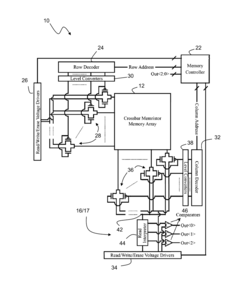
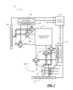
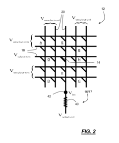
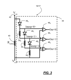
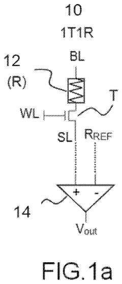
- A resistive memory structure with an interpretation circuit that includes active and passive devices connected in series to interpret voltage levels at an electrical node, allowing for accurate determination of resistive states without significant peripheral circuitry, and a method involving specific voltage biasing schemes to minimize resistance changes during operations.
Write method for differential resistive memories
PatentActiveUS12119059B2
Innovation
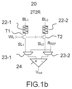
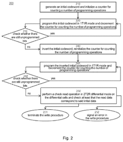
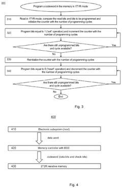
- A write method for 2T2R resistive memories that alternates between 1T1R mode programming and check read operations, incrementing or decrementing a counter for each programming step, and performs a final check in 2T2R differential mode to ensure data accuracy, reducing the number of write operations and energy consumption.
Performance Benchmarking Against Competing Technologies
In evaluating Resistive RAM (ReRAM) against competing memory technologies, comprehensive performance benchmarking reveals significant comparative advantages and limitations. ReRAM demonstrates superior write endurance of 10^6-10^12 cycles compared to NAND Flash's 10^3-10^5 cycles, positioning it favorably for write-intensive applications. However, it falls short of DRAM's virtually unlimited endurance (>10^15 cycles).
Power consumption metrics indicate ReRAM consumes approximately 0.1-1 pJ per bit operation, substantially lower than DRAM's 2-5 pJ and NAND Flash's 10-100 pJ for write operations. This energy efficiency represents a critical advantage in mobile and IoT applications where power constraints are significant design factors.
Access speed benchmarks position ReRAM between volatile and non-volatile alternatives, with read latencies of 10-100 ns compared to DRAM's 10-50 ns and NAND Flash's microsecond-range latencies. Write speeds follow similar patterns, making ReRAM a compelling middle-ground solution that balances performance with non-volatility.
Density and scalability metrics demonstrate ReRAM's potential for high-density storage with cell sizes approaching 4F² in crossbar architectures, comparable to 3D NAND but with simpler fabrication requirements. Multi-level cell capabilities further enhance this density advantage, though reliability challenges remain at advanced nodes.
Retention characteristics show ReRAM maintaining data integrity for 10+ years at 85°C, matching or exceeding other non-volatile technologies while significantly outperforming volatile alternatives that require constant power for data retention.
Cost analysis reveals ReRAM currently commands higher per-gigabyte pricing than mature technologies like NAND Flash, but demonstrates favorable trajectories as manufacturing processes mature. Integration compatibility with standard CMOS processes provides additional cost advantages compared to specialized memory fabrication requirements.
Reliability benchmarks highlight ReRAM's resistance to radiation effects and electromagnetic interference compared to charge-based storage technologies, though variability in switching behavior remains a challenge requiring sophisticated error correction mechanisms.
These comparative metrics collectively position ReRAM as a promising technology for specific application domains requiring balanced performance, particularly in edge computing, automotive systems, and neuromorphic applications where its unique characteristics align with operational requirements.
Manufacturing Scalability and Cost Analysis
Manufacturing scalability represents a critical factor in the commercial viability of memory technologies. Resistive RAM (RRAM) demonstrates significant advantages in this domain compared to conventional and emerging memory alternatives. The fabrication process for RRAM utilizes standard CMOS-compatible materials and processes, enabling integration with existing semiconductor manufacturing infrastructure without requiring substantial capital investments in specialized equipment.
When examining the manufacturing complexity, RRAM exhibits a relatively simple structure consisting of a metal-insulator-metal stack, which can be fabricated with fewer process steps compared to technologies like 3D NAND or MRAM. This structural simplicity translates directly to reduced manufacturing costs and higher production yields. Industry analyses indicate that RRAM fabrication requires approximately 30-40% fewer mask layers than comparable high-performance memory technologies.
The scalability of RRAM extends to dimensional scaling as well. Current research demonstrates functional RRAM cells at nodes below 10nm, with theoretical scaling potential extending to the sub-5nm regime. This compares favorably to DRAM, which faces significant scaling challenges below 15nm, and even against other emerging technologies like PCM, which encounters crystallization issues at extreme dimensions.
From a cost perspective, RRAM presents an attractive value proposition. The cost-per-bit metric for RRAM is projected to decrease more rapidly than competing technologies due to its compatibility with crossbar architectures, which maximize storage density. Economic models suggest that at high-volume production, RRAM could achieve costs approaching $0.01 per gigabyte, positioning it competitively against established technologies.
Manufacturing yield represents another crucial economic factor. The relatively simple structure of RRAM cells contributes to higher manufacturing yields compared to technologies with more complex structures or stringent material requirements. Current industry data indicates RRAM yield rates of 85-90% in pilot production environments, with expectations of reaching 95%+ in mature manufacturing processes.
The 3D integration capability of RRAM further enhances its manufacturing economics. Unlike conventional planar memory architectures, RRAM can be stacked in multiple layers, significantly increasing storage density without proportionally increasing die size. This vertical scaling approach allows manufacturers to maximize the number of bits per wafer, thereby reducing the effective cost per bit while maintaining reasonable manufacturing complexity.
Unlock deeper insights with Patsnap Eureka Quick Research — get a full tech report to explore trends and direct your research. Try now!
Generate Your Research Report Instantly with AI Agent
Supercharge your innovation with Patsnap Eureka AI Agent Platform!