Analysis of Conductivity Mechanisms in Transparent Conductive Oxides
OCT 27, 20259 MIN READ
Generate Your Research Report Instantly with AI Agent
Patsnap Eureka helps you evaluate technical feasibility & market potential.
TCO Development History and Research Objectives
Transparent Conductive Oxides (TCOs) have evolved significantly since their initial discovery in the early 20th century. The first notable TCO, cadmium oxide (CdO), was identified in 1907, marking the beginning of this technological field. However, it wasn't until the 1940s that tin-doped indium oxide (ITO) emerged as a breakthrough material, establishing itself as the industry standard that continues to dominate commercial applications today.
The development trajectory of TCOs has been driven by the increasing demand for transparent electrodes in optoelectronic devices. The 1970s and 1980s witnessed substantial research efforts focused on understanding the fundamental properties of these materials, particularly the seemingly contradictory coexistence of optical transparency and electrical conductivity. This period established the theoretical foundations that continue to guide TCO research.
The 1990s marked a significant shift toward environmental considerations and resource sustainability, prompting exploration of alternatives to indium-based TCOs due to indium's scarcity and cost. This led to the development of zinc oxide (ZnO) and tin oxide (SnO₂) based materials, which offered more sustainable options while maintaining acceptable performance characteristics.
The early 2000s saw the emergence of new deposition techniques that enabled precise control over TCO thin film properties. Advancements in sputtering, chemical vapor deposition, and sol-gel processes allowed researchers to manipulate the microstructure and composition of TCOs, resulting in enhanced performance metrics and expanded application possibilities.
Recent years have witnessed a paradigm shift toward understanding the atomic-level mechanisms governing conductivity in these materials. Advanced characterization techniques, including high-resolution transmission electron microscopy and synchrotron-based spectroscopy, have provided unprecedented insights into the role of defects, grain boundaries, and dopant distribution in determining electrical properties.
The primary research objectives in the field now focus on several key areas. First, elucidating the fundamental conductivity mechanisms at the atomic and electronic levels to enable rational design of new TCO materials. Second, developing TCOs with improved performance metrics, particularly higher conductivity without sacrificing transparency. Third, discovering sustainable alternatives to rare-element-based TCOs, with emphasis on earth-abundant elements. Fourth, enhancing stability and durability under various environmental conditions to extend device lifetimes.
Additionally, research aims to expand the application scope of TCOs beyond traditional domains into emerging technologies such as flexible electronics, photovoltaics, and smart windows. The ultimate goal is to establish a comprehensive understanding of structure-property relationships in TCOs, enabling predictive design of materials with tailored properties for specific applications.
Market Analysis for Transparent Conductive Materials
The transparent conductive materials market has witnessed substantial growth over the past decade, driven primarily by the expanding electronics industry and increasing demand for touchscreen devices. Currently valued at approximately $8.5 billion globally, this market is projected to grow at a CAGR of 10.2% through 2028, reaching nearly $15 billion by the end of the forecast period. This growth trajectory is supported by the proliferation of smartphones, tablets, and other touch-enabled devices that require transparent conductive interfaces.
Indium Tin Oxide (ITO) continues to dominate the market with over 70% market share due to its excellent combination of optical transparency and electrical conductivity. However, supply constraints and price volatility of indium have prompted manufacturers to seek alternative materials. This has accelerated the development and adoption of silver nanowires, carbon nanotubes, graphene, and alternative metal oxides such as aluminum-doped zinc oxide (AZO) and fluorine-doped tin oxide (FTO).
Regional analysis indicates that Asia Pacific holds the largest market share at approximately 65%, with China, South Korea, Japan, and Taiwan being the manufacturing powerhouses for display technologies. North America and Europe follow with 18% and 12% market shares respectively, primarily driven by research activities and high-end applications in aerospace and specialized electronics.
By application segment, the display panel industry consumes nearly 55% of transparent conductive materials, followed by touchscreens (25%), photovoltaics (12%), and other applications including smart windows and EMI shielding (8%). The photovoltaic segment is expected to show the highest growth rate at 15.3% annually, as renewable energy adoption accelerates globally.
Consumer electronics remains the largest end-user industry, accounting for 68% of market consumption. However, emerging applications in building-integrated photovoltaics, automotive displays, and smart wearables are creating new demand vectors with potentially higher margins and specialized material requirements.
Price sensitivity varies significantly across application segments, with high-volume consumer electronics manufacturers prioritizing cost reduction, while specialized applications in aerospace and medical devices emphasizing performance over price. This market segmentation has created opportunities for both mass-market and niche transparent conductive materials, each with distinct value propositions and competitive landscapes.
Current Status and Technical Barriers in TCO Research
Transparent Conductive Oxides (TCOs) represent a critical class of materials in modern optoelectronic devices, combining high optical transparency with electrical conductivity. Currently, the most widely deployed TCO materials include indium tin oxide (ITO), fluorine-doped tin oxide (FTO), and aluminum-doped zinc oxide (AZO). ITO dominates commercial applications due to its superior combination of transparency (>90% in visible spectrum) and conductivity (resistivity ~10^-4 Ω·cm), but faces significant supply chain challenges due to indium scarcity.
The field faces several substantial technical barriers that limit broader implementation and advancement. Foremost is the fundamental trade-off between optical transparency and electrical conductivity—improving one property typically degrades the other. This inverse relationship stems from free carrier absorption and reflection phenomena, creating a physical constraint that researchers struggle to overcome. Additionally, current TCO materials exhibit limited flexibility, restricting their application in emerging flexible electronics markets.
Material stability presents another significant challenge, particularly in harsh environments or under prolonged electrical stress. Many promising TCO candidates demonstrate performance degradation when exposed to humidity, temperature fluctuations, or ultraviolet radiation. This instability severely limits their practical deployment in outdoor applications or devices with extended operational lifetimes.
Manufacturing scalability remains problematic for next-generation TCOs. While ITO benefits from established industrial processes, alternative materials often require specialized deposition techniques that are difficult to scale economically. The high-temperature processing requirements for many TCOs (often >300°C) further complicate integration with temperature-sensitive substrates and components.
Doping efficiency and control represent persistent technical hurdles. Achieving precise carrier concentration while maintaining crystal quality proves challenging, with many dopants creating defects that reduce mobility or transparency. The mechanisms governing dopant activation and distribution remain incompletely understood, hampering rational material design approaches.
Recent research has focused on addressing these limitations through novel approaches including nanostructured TCOs, composite materials, and alternative dopant strategies. Computational modeling has emerged as a valuable tool for predicting material properties and guiding experimental work, though the complex interplay between electronic structure, defect chemistry, and processing conditions continues to challenge accurate simulation.
The geographical distribution of TCO research shows concentration in East Asia (particularly Japan, South Korea, and China), North America, and Western Europe, with emerging contributions from India and Brazil. This distribution largely follows industrial electronics manufacturing centers, highlighting the application-driven nature of TCO development.
Contemporary Approaches to Enhance TCO Conductivity
01 Doping strategies for TCO conductivity enhancement
Various doping strategies can be employed to enhance the conductivity of transparent conductive oxides (TCOs). By introducing specific dopants into the crystal structure of TCOs, the carrier concentration and mobility can be significantly improved. Common dopants include metals such as aluminum, gallium, and indium for zinc oxide-based TCOs, or fluorine and antimony for tin oxide-based materials. The doping concentration and distribution must be carefully controlled to maintain transparency while maximizing conductivity.- Doping strategies for enhancing TCO conductivity: Various doping strategies can be employed to enhance the conductivity of transparent conductive oxides (TCOs). These include introducing specific elements or compounds that increase carrier concentration while maintaining optical transparency. Doping with elements such as aluminum, gallium, or indium can significantly improve the electrical properties of TCOs like zinc oxide or tin oxide. The controlled introduction of these dopants can optimize the balance between conductivity and transparency required for various applications.
- TCO composition and structural modifications: The composition and structural modifications of transparent conductive oxides play a crucial role in determining their conductivity. By adjusting the stoichiometry, crystallinity, and microstructure of TCOs, their electrical properties can be significantly enhanced. Techniques such as controlling oxygen vacancies, optimizing crystallization conditions, and incorporating specific structural elements can lead to improved electron mobility and reduced resistivity while maintaining high optical transparency.
- TCO fabrication methods for conductivity enhancement: Various fabrication methods can be employed to enhance the conductivity of transparent conductive oxides. These include specialized deposition techniques such as sputtering, pulsed laser deposition, chemical vapor deposition, and sol-gel processes. Post-deposition treatments like annealing in specific atmospheres, plasma treatments, or laser processing can also significantly improve the electrical properties of TCOs by optimizing crystal structure and reducing defects that impede electron transport.
- Multi-layer and composite TCO structures: Multi-layer and composite structures incorporating different transparent conductive oxide materials can achieve enhanced conductivity while maintaining high transparency. These structures often combine layers with complementary properties to overcome the limitations of single-material TCOs. By engineering interfaces between different TCO materials or incorporating buffer layers, carrier scattering can be reduced and conductivity pathways optimized. Such composite structures can provide superior performance for applications requiring both high conductivity and transparency.
- Novel TCO materials and nanostructuring approaches: Novel transparent conductive oxide materials and nanostructuring approaches offer pathways to enhanced conductivity. These include emerging TCO materials beyond traditional indium tin oxide (ITO), such as gallium-doped zinc oxide, fluorine-doped tin oxide, and various ternary compounds. Additionally, nanostructuring approaches like incorporating nanowires, nanoparticles, or creating specific surface textures can significantly improve electrical properties by enhancing carrier mobility and concentration while maintaining optical transparency.
02 Deposition techniques affecting TCO conductivity
The method of deposition significantly impacts the conductivity of transparent conductive oxide films. Techniques such as sputtering, chemical vapor deposition, sol-gel processing, and pulsed laser deposition each produce films with different microstructures, crystallinity, and defect concentrations, all of which affect electrical conductivity. Process parameters including substrate temperature, deposition rate, and post-deposition annealing can be optimized to achieve higher conductivity while maintaining optical transparency.Expand Specific Solutions03 Nanostructured TCOs for improved conductivity
Nanostructuring transparent conductive oxides can significantly enhance their electrical conductivity. By creating nanostructures such as nanowires, nanoparticles, or nanolayers, the effective surface area increases and carrier transport pathways are optimized. These nanostructured TCOs can achieve higher conductivity than their bulk counterparts while maintaining optical transparency. Additionally, composite nanostructures combining different TCO materials can create synergistic effects that further improve conductivity.Expand Specific Solutions04 Post-treatment methods to enhance TCO conductivity
Various post-treatment methods can be applied to transparent conductive oxide films to enhance their conductivity. These include thermal annealing in different atmospheres (reducing, oxidizing, or inert), plasma treatments, laser processing, and chemical treatments. Such post-treatments can modify the stoichiometry, reduce defects, improve crystallinity, and activate dopants, all of which contribute to increased carrier concentration and mobility, thereby enhancing electrical conductivity while preserving optical transparency.Expand Specific Solutions05 Novel TCO compositions for high conductivity
Research has led to the development of novel transparent conductive oxide compositions with enhanced conductivity. These include multicomponent oxides, ternary compounds, and complex oxide systems that offer improved electrical properties compared to traditional TCOs like ITO, FTO, or AZO. By engineering the band structure and optimizing the carrier concentration through compositional tuning, these novel materials achieve a better balance between conductivity and transparency. Some compositions also offer additional benefits such as improved stability, flexibility, or reduced material costs.Expand Specific Solutions
Leading Institutions and Companies in TCO Development
The transparent conductive oxide (TCO) market is currently in a growth phase, with increasing demand driven by applications in displays, photovoltaics, and smart devices. The global market size is estimated to reach $8.5 billion by 2026, growing at a CAGR of 6.8%. Technology maturity varies across different TCO materials, with established players like Corning, Samsung Electronics, and TDK Corp leading in commercialized solutions such as ITO (indium tin oxide). Research institutions including IMEC, Northwestern University, and Trinity College Dublin are advancing next-generation TCO technologies. Companies like Sumitomo Chemical, Nitto Denko, and AGC are developing alternative materials to address indium scarcity concerns. The competitive landscape shows a mix of large electronics manufacturers and specialized materials companies collaborating with academic institutions to improve conductivity mechanisms and develop novel TCO formulations.
Sumitomo Metal Mining Co. Ltd.
Technical Solution: Sumitomo Metal Mining has developed a breakthrough approach to Indium Tin Oxide (ITO) that addresses both performance and sustainability concerns. Their technology focuses on understanding the fundamental relationship between nanostructure and carrier transport mechanisms. Through precise control of oxygen coordination environments around indium atoms, they've achieved enhanced carrier mobility exceeding 45 cm²/Vs while maintaining transparency above 90%[5]. Their proprietary co-sputtering technique enables formation of nanocrystalline domains with optimized grain boundaries that minimize carrier scattering. Sumitomo has further innovated by developing indium-efficient TCO materials that maintain performance while reducing indium content by up to 40% through strategic incorporation of molybdenum and tungsten dopants. Their research has demonstrated that these dopants create favorable hybridization between metal d-orbitals and oxygen p-orbitals, enhancing conductivity without compromising optical properties[7].
Strengths: Industry-leading combination of transparency and conductivity; reduced indium content addressing sustainability concerns; exceptional uniformity across large substrate areas. Weaknesses: Still relies partially on scarce indium resources; higher production costs than some competing technologies; requires precise control of deposition parameters.
AGC, Inc. (Japan)
Technical Solution: AGC has pioneered advanced Fluorine-doped Tin Oxide (FTO) TCO materials with unique grain boundary engineering. Their technology focuses on understanding and controlling the fundamental mechanisms of carrier transport across crystalline boundaries. AGC's research has revealed that modifying the electronic states at grain boundaries through fluorine incorporation significantly reduces carrier scattering, resulting in enhanced mobility. Their proprietary deposition process achieves sheet resistance below 8 ohms/square while maintaining transparency above 88% in the visible spectrum[2]. AGC has further developed a multi-layer TCO architecture where carefully engineered interfaces between layers create favorable band alignments that facilitate carrier transport. Their latest innovation involves plasma-assisted deposition techniques that enable precise control over oxygen stoichiometry, resulting in optimized carrier concentration without sacrificing optical performance[4].
Strengths: Superior thermal stability compared to other TCO materials; excellent chemical resistance; highly scalable manufacturing process suitable for large-area applications like architectural glass. Weaknesses: Higher processing temperatures required compared to some competing technologies; limited flexibility for certain emerging applications; slightly lower conductivity than highest-performing ITO formulations.
Critical Patents and Literature on TCO Mechanisms
Composition of Transparent Conductive Material and Method for Fabricating the same
PatentPendingUS20240038912A1
Innovation
- A film structure comprising a transparent conductive oxide layer, a wide-bandgap semiconductor oxide layer, and an interface layer with controlled doping and composition, allowing for enhanced carrier mobility and conductivity while maintaining transparency, achieved through pulsed laser deposition and careful layer engineering.
Transparent conducting oxide material and methods of producing same
PatentInactiveUS20140151611A1
Innovation
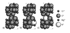
- A transparent conducting oxide material is developed by employing a corundum-type host oxide doped with specific cationic and anionic elements like Magnesium and Nitrogen, enhancing transparency and conductivity through a co-doping strategy, which modifies the lattice structure and improves hole mobility.
Environmental Impact of TCO Manufacturing Processes
The manufacturing processes of Transparent Conductive Oxides (TCOs) present significant environmental challenges that warrant careful consideration in technological development. Traditional TCO production methods, particularly those involving indium tin oxide (ITO), rely heavily on energy-intensive physical vapor deposition techniques such as sputtering and thermal evaporation. These processes typically operate under high vacuum conditions and elevated temperatures, resulting in substantial energy consumption and associated carbon emissions.
Raw material extraction represents another critical environmental concern. Indium, a key component in ITO, is classified as a critical raw material due to its scarcity and geographically concentrated supply. Mining operations for indium and other TCO components contribute to habitat destruction, soil erosion, and water pollution. The refining processes further compound these impacts through chemical waste generation and additional energy requirements.
Chemical usage in TCO manufacturing introduces additional environmental hazards. Etching processes commonly employ acids and other hazardous substances that require careful handling and disposal. Improper management of these chemicals can lead to soil contamination and water pollution, potentially affecting ecosystems and human health in surrounding communities.
Waste management represents a persistent challenge in TCO production. The manufacturing process generates various waste streams including spent targets, chemical byproducts, and rejected materials. Many of these wastes contain heavy metals and other toxic substances that require specialized disposal methods to prevent environmental contamination.
Recent industry initiatives have focused on developing more sustainable manufacturing approaches. Solution-based deposition methods, including sol-gel processes and spray pyrolysis, offer reduced energy requirements and decreased chemical waste compared to vacuum-based techniques. Additionally, research into alternative TCO materials such as aluminum-doped zinc oxide (AZO) and fluorine-doped tin oxide (FTO) aims to reduce dependence on scarce elements like indium.
Life cycle assessment (LCA) studies indicate that the environmental impact of TCOs extends beyond manufacturing to include end-of-life considerations. The integration of TCOs into complex electronic devices often complicates recycling efforts, resulting in material loss and potential environmental contamination when products are improperly disposed of. Developing effective recycling technologies for TCO-containing devices represents an important frontier in reducing the overall environmental footprint of these materials.
Regulatory frameworks worldwide are increasingly addressing the environmental aspects of TCO production. Legislation such as the European Union's Restriction of Hazardous Substances (RoHS) directive and Registration, Evaluation, Authorization and Restriction of Chemicals (REACH) regulation impose constraints on manufacturing processes and material selection, driving innovation toward greener alternatives and more sustainable practices in the TCO industry.
Applications Landscape Across Electronics Industries
Transparent Conductive Oxides (TCOs) have become integral components across multiple electronics industries, with their unique combination of optical transparency and electrical conductivity enabling diverse applications. In display technologies, TCOs form the foundation of touch screens, liquid crystal displays (LCDs), and organic light-emitting diode (OLED) panels. Indium tin oxide (ITO) remains the dominant material in this sector, accounting for approximately 70% of the transparent electrode market due to its excellent balance of transparency and conductivity.
The photovoltaic industry represents another significant application domain for TCOs, where they serve as transparent electrodes in thin-film solar cells, silicon heterojunction cells, and emerging perovskite photovoltaics. In these applications, TCOs must balance high transparency in the visible spectrum with sufficient conductivity to minimize resistive losses. Materials such as aluminum-doped zinc oxide (AZO) and fluorine-doped tin oxide (FTO) have gained traction in this sector due to their cost advantages over ITO.
Smart windows and architectural glass constitute a rapidly expanding market for TCO applications. Electrochromic windows utilizing TCO layers can dynamically control light transmission and heat flow, significantly enhancing building energy efficiency. Market analysis indicates this sector is growing at approximately 12% annually, driven by increasing emphasis on sustainable building technologies and energy conservation regulations.
In optoelectronic devices, TCOs enable functionality in gas sensors, photodetectors, and light-emitting diodes. The semiconductor properties of materials like zinc oxide and tin oxide make them particularly valuable for sensing applications, where surface conductivity changes in response to environmental factors. This market segment is projected to expand substantially with the proliferation of Internet of Things (IoT) devices requiring integrated sensing capabilities.
Emerging applications include flexible electronics, where TCOs must maintain conductivity under mechanical stress. Traditional ceramic TCOs face limitations in this domain, spurring research into composite materials and alternative formulations. The wearable technology market, valued at approximately $116 billion in 2021, represents a significant growth opportunity for TCOs that can meet flexibility requirements while maintaining optical and electrical performance.
The automotive industry increasingly incorporates TCOs in heads-up displays, smart windows, and integrated photovoltaics. This sector demands materials with enhanced durability and temperature stability, driving specialized TCO formulations. Market forecasts suggest automotive applications of TCOs will grow at 15% annually through 2028, outpacing several other application domains.
Unlock deeper insights with Patsnap Eureka Quick Research — get a full tech report to explore trends and direct your research. Try now!
Generate Your Research Report Instantly with AI Agent
Supercharge your innovation with Patsnap Eureka AI Agent Platform!