Analysis of Transparent Conductive Oxides in Optical Devices
OCT 27, 20259 MIN READ
Generate Your Research Report Instantly with AI Agent
Patsnap Eureka helps you evaluate technical feasibility & market potential.
TCO Technology Background and Objectives
Transparent Conductive Oxides (TCOs) have emerged as critical materials in modern optoelectronic devices, evolving significantly since their initial development in the early 20th century. The journey of TCO materials began with the discovery of cadmium oxide's conductive properties in 1907, followed by tin oxide in the 1940s. However, the field experienced transformative growth with the introduction of indium tin oxide (ITO) in the 1960s, which remains the industry standard despite ongoing challenges.
The technological evolution of TCOs has been driven by the increasing demand for devices that require both optical transparency and electrical conductivity—properties that are inherently contradictory in most materials. This unique combination enables TCOs to serve as essential components in displays, photovoltaics, smart windows, and emerging flexible electronics, creating a technological foundation for numerous high-value applications.
Current TCO development focuses on addressing several critical objectives. First, reducing dependence on indium, a scarce and expensive element that constitutes the primary component of ITO, represents an urgent priority. Second, enhancing performance metrics—particularly the figure of merit that balances conductivity and transparency—continues to drive research efforts. Third, developing TCOs compatible with flexible substrates has become increasingly important as the electronics industry shifts toward bendable and wearable devices.
The technological trajectory indicates a move toward more sustainable and abundant materials, with zinc oxide, fluorine-doped tin oxide, and various ternary compounds gaining significant research attention. Additionally, novel deposition techniques such as atomic layer deposition and solution processing are being explored to enable low-temperature processing compatible with temperature-sensitive substrates.
Recent breakthroughs in nanostructured TCOs have demonstrated potential for surpassing the performance limitations of traditional materials. These advanced structures manipulate light-matter interactions at the nanoscale, potentially offering superior optical and electrical properties while using less material. Concurrently, the integration of TCOs with emerging materials like graphene and conductive polymers represents a promising frontier for hybrid systems with enhanced functionality.
The overarching goal of current TCO research centers on developing materials that maintain excellent optical transparency (>90% in the visible spectrum) while achieving sheet resistances below 10 ohms/square, all while using earth-abundant elements and environmentally friendly processing methods. These objectives align with broader industry trends toward sustainable electronics and advanced optical devices with enhanced performance characteristics.
Market Analysis for TCO-based Optical Devices
The global market for Transparent Conductive Oxide (TCO) based optical devices has witnessed substantial growth in recent years, driven primarily by increasing demand for touchscreen displays, photovoltaic cells, and smart windows. The market value reached approximately $8.7 billion in 2022 and is projected to grow at a compound annual growth rate (CAGR) of 6.8% through 2028, potentially reaching $13.5 billion by the end of the forecast period.
Consumer electronics remains the dominant application segment, accounting for nearly 45% of the total market share. This is largely attributed to the widespread adoption of smartphones, tablets, and wearable devices that utilize TCO materials in their display technologies. Indium Tin Oxide (ITO) continues to be the market leader among TCO materials, representing about 70% of the market despite ongoing efforts to develop alternatives due to indium's limited supply and price volatility.
The photovoltaic sector represents the fastest-growing application segment with a CAGR of 9.2%, as TCO materials are critical components in thin-film solar cells and emerging perovskite solar technologies. The building and construction industry is also showing increased interest in TCO-based smart windows and energy-efficient glazing solutions, with market penetration expected to double in the next five years.
Regionally, Asia-Pacific dominates the market with approximately 65% share, primarily due to the concentration of electronics manufacturing in countries like China, South Korea, Japan, and Taiwan. North America and Europe follow with 18% and 14% market shares respectively, with particular growth in specialized applications such as automotive displays and aerospace components.
Key market drivers include technological advancements in flexible electronics, increasing environmental regulations favoring energy-efficient solutions, and growing investment in renewable energy infrastructure. The push toward Internet of Things (IoT) devices and smart home technologies is creating new application avenues for TCO-based optical devices.
Market challenges include supply chain vulnerabilities for critical raw materials, particularly indium, and intense price competition from emerging economies. Additionally, technical limitations such as brittleness in flexible applications and performance degradation under certain conditions continue to constrain market expansion in specific segments.
Customer demand is increasingly shifting toward TCO materials that offer higher transparency, lower resistivity, improved flexibility, and enhanced durability. This trend is pushing manufacturers to invest in research and development of next-generation TCO materials such as aluminum-doped zinc oxide (AZO), fluorine-doped tin oxide (FTO), and various nanocomposite structures that could potentially address current limitations while reducing dependency on scarce materials.
Current Status and Challenges in TCO Development
Transparent Conductive Oxides (TCOs) have become indispensable components in modern optical and optoelectronic devices. Currently, the global TCO market is dominated by Indium Tin Oxide (ITO), which accounts for approximately 85% of all TCO applications due to its excellent combination of optical transparency and electrical conductivity. However, the scarcity and rising cost of indium have prompted intensive research into alternative materials.
The current development of TCOs faces several significant challenges. First, there exists a fundamental trade-off between optical transparency and electrical conductivity. As carrier concentration increases to improve conductivity, free carrier absorption and reflection increase, reducing optical transparency in the visible and near-infrared regions. This intrinsic contradiction limits the performance of conventional TCO materials in high-end applications requiring both properties simultaneously.
Material stability presents another major challenge, particularly for applications in harsh environments or those requiring long-term reliability. Many promising TCO candidates exhibit degradation when exposed to humidity, high temperatures, or mechanical stress. For instance, zinc oxide-based TCOs often suffer from environmental instability despite their attractive optoelectronic properties and lower cost compared to ITO.
Manufacturing scalability remains a significant hurdle for emerging TCO technologies. While laboratory-scale production has demonstrated promising results for materials such as fluorine-doped tin oxide (FTO) and aluminum-doped zinc oxide (AZO), transitioning these processes to industrial-scale production while maintaining uniform properties across large areas presents considerable technical difficulties. Current deposition techniques like sputtering, chemical vapor deposition, and sol-gel methods each have limitations regarding throughput, material quality, or cost-effectiveness.
The geographical distribution of TCO research and production capabilities shows significant concentration in East Asia, particularly Japan, South Korea, and China, which collectively account for over 60% of TCO-related patents filed in the past decade. North America and Europe maintain strong positions in fundamental research but lag in commercial production capacity.
Recent technological breakthroughs include the development of amorphous TCOs with reduced grain boundary scattering, which has enabled higher electron mobility without sacrificing transparency. Additionally, composite and multilayer TCO structures have shown promise in overcoming the transparency-conductivity trade-off by engineering the interface properties between different materials.
The integration of TCOs with emerging technologies such as flexible electronics and photovoltaics introduces additional challenges related to mechanical flexibility, adhesion to polymer substrates, and compatibility with low-temperature processing. These applications demand TCOs that can maintain their optoelectronic properties under bending and stretching conditions, a requirement that conventional brittle oxide materials struggle to meet.
Current TCO Material Solutions and Applications
01 Indium-based transparent conductive oxides
Indium-based materials, particularly indium tin oxide (ITO), are widely used as transparent conductive oxides in various electronic applications. These materials offer excellent electrical conductivity while maintaining high optical transparency in the visible spectrum. Research focuses on optimizing deposition methods, improving conductivity, and enhancing durability of these films for applications in displays, touch screens, and photovoltaic devices.- Composition and structure of transparent conductive oxides: Transparent conductive oxides (TCOs) are materials that combine optical transparency with electrical conductivity. These materials typically consist of metal oxides such as indium tin oxide (ITO), zinc oxide (ZnO), or tin oxide (SnO2) that have been doped with specific elements to enhance their electrical properties while maintaining optical transparency. The composition and crystal structure of these materials significantly influence their performance characteristics, including conductivity, transparency, and stability.
- Fabrication methods for transparent conductive oxide films: Various deposition techniques are employed to fabricate transparent conductive oxide films, including sputtering, chemical vapor deposition, sol-gel processes, and atomic layer deposition. These methods allow for precise control over film thickness, composition, and microstructure, which directly impact the electrical and optical properties of the resulting films. Post-deposition treatments such as annealing can further enhance the performance of these materials by improving crystallinity and reducing defects.
- Applications in optoelectronic devices: Transparent conductive oxides are widely used in various optoelectronic devices including solar cells, light-emitting diodes (LEDs), flat panel displays, and touch screens. Their unique combination of optical transparency and electrical conductivity makes them ideal for applications requiring transparent electrodes. In solar cells, TCOs serve as front electrodes that allow light to pass through while collecting generated charge carriers, thereby improving device efficiency.
- Novel TCO materials and doping strategies: Research on transparent conductive oxides focuses on developing new materials and doping strategies to overcome limitations of traditional TCOs such as indium scarcity and brittleness. Alternative materials include aluminum-doped zinc oxide (AZO), fluorine-doped tin oxide (FTO), and more complex multi-component oxides. Various doping elements and concentrations are explored to optimize the balance between electrical conductivity and optical transparency, while also improving other properties such as chemical stability and mechanical flexibility.
- TCO integration in flexible and next-generation electronics: Integration of transparent conductive oxides into flexible and next-generation electronic devices presents unique challenges and opportunities. Techniques for depositing TCOs on flexible substrates at low temperatures, creating patterned TCO structures, and ensuring mechanical durability under bending stress are being developed. Hybrid structures combining TCOs with other materials such as graphene, metal nanowires, or conductive polymers are also being explored to create transparent electrodes with enhanced performance characteristics for emerging applications like wearable electronics and flexible displays.
02 Zinc oxide-based transparent conductive materials
Zinc oxide (ZnO) based transparent conductive materials, often doped with elements like aluminum or gallium, represent an important alternative to indium-based TCOs. These materials offer good transparency and conductivity with the advantages of lower cost, earth abundance, and environmental friendliness. Various deposition techniques and post-treatment methods are employed to enhance their electrical and optical properties for use in thin-film solar cells and optoelectronic devices.Expand Specific Solutions03 Fabrication methods for transparent conductive oxide films
Various fabrication methods are employed to produce high-quality transparent conductive oxide films with optimized properties. These include physical vapor deposition techniques such as sputtering, pulsed laser deposition, and thermal evaporation, as well as chemical methods like sol-gel processing and chemical vapor deposition. Post-deposition treatments including annealing in different atmospheres are often used to improve crystallinity, reduce defects, and enhance electrical conductivity while maintaining optical transparency.Expand Specific Solutions04 Novel TCO compositions and nanostructured materials
Research on novel transparent conductive oxide compositions focuses on developing materials with improved performance characteristics or reduced reliance on scarce elements. This includes multicomponent oxides, nanostructured materials, and composite systems that can achieve enhanced electrical conductivity without sacrificing optical transparency. Nanostructured TCOs, including nanowires, nanoparticles, and patterned films, offer unique advantages in terms of flexibility, surface area, and tunable properties for next-generation electronic and optoelectronic applications.Expand Specific Solutions05 TCO applications in photovoltaics and display technologies
Transparent conductive oxides play crucial roles in photovoltaic devices and display technologies. In solar cells, TCOs serve as transparent electrodes that allow light to pass through while collecting generated charge carriers. For display applications, TCOs function as transparent electrodes in technologies such as LCDs, OLEDs, and touch panels. Research focuses on optimizing TCO properties specifically for these applications, including work function matching, interface engineering, and enhancing long-term stability under operating conditions.Expand Specific Solutions
Key Industry Players in TCO Manufacturing
The transparent conductive oxides (TCO) market in optical devices is currently in a growth phase, with increasing demand driven by the expanding optoelectronics industry. The global market size is projected to reach significant value due to applications in displays, photovoltaics, and smart windows. Technologically, TCOs are advancing from traditional indium tin oxide (ITO) to alternative materials. Leading players demonstrate varying levels of technological maturity: established manufacturers like Samsung Electronics, LG Display, and Corning have commercialized products, while research institutions such as ICFO, Peking University, and ITRI are developing next-generation TCO materials. Micron Technology and Eastman Kodak are leveraging TCOs for specialized applications, while companies like Cambrios Technologies are pioneering silver nanowire alternatives, indicating a competitive landscape transitioning toward more sustainable and higher-performance solutions.
Corning, Inc.
Technical Solution: Corning has developed advanced transparent conductive oxide (TCO) materials, particularly focusing on indium tin oxide (ITO) alternatives. Their proprietary Antimony Tin Oxide (ATO) technology offers enhanced durability while maintaining high transparency in the visible spectrum. Corning's approach integrates TCO materials with their glass substrates through specialized sputtering techniques that create uniform, defect-free coatings with controlled thickness down to nanometer precision[1]. Their recent innovations include flexible TCO films that can withstand over 200,000 bending cycles without significant conductivity loss, achieved through a unique multilayer architecture that distributes mechanical stress. Corning has also pioneered low-temperature deposition methods that enable TCO application on temperature-sensitive substrates, expanding potential applications in flexible displays and photovoltaics[2]. Their materials demonstrate transmittance exceeding 90% across visible wavelengths while maintaining sheet resistance below 10 ohms/square, positioning them as industry leaders in high-performance optical device components.
Strengths: Exceptional integration capabilities with glass substrates, superior mechanical durability, and established manufacturing infrastructure for large-scale production. Weaknesses: Higher production costs compared to standard ITO solutions, and some formulations require rare earth elements that face supply chain constraints.
Samsung Electronics Co., Ltd.
Technical Solution: Samsung has developed a comprehensive TCO technology portfolio centered around zinc-based compounds for optical device applications. Their flagship Aluminum-doped Zinc Oxide (AZO) technology achieves optical transparency above 85% while maintaining electrical conductivity comparable to traditional ITO but at significantly reduced costs[3]. Samsung's proprietary deposition process enables precise control of film microstructure, resulting in enhanced carrier mobility exceeding 40 cm²/Vs. Their TCO materials are integrated into OLED displays through a specialized multi-layer architecture that optimizes both optical and electrical performance while minimizing reflection at interfaces. Samsung has also pioneered hybrid TCO structures combining different materials to achieve optimal performance across various device requirements. Recent innovations include room-temperature processed TCOs using solution-based methods that reduce manufacturing energy consumption by approximately 40% compared to conventional vacuum deposition techniques[4]. Their TCO technology roadmap includes development of self-healing conductive films that can recover from mechanical damage, addressing durability concerns in flexible display applications.
Strengths: Vertical integration capabilities from material development to device manufacturing, extensive IP portfolio in TCO applications for displays, and cost-effective manufacturing processes. Weaknesses: Some formulations show performance degradation under high humidity conditions, and certain proprietary compounds have limited compatibility with industry-standard processing equipment.
Critical Patents and Research in TCO Technology
Atomic layer deposited titanium-doped indium oxide films
PatentActiveUS7582161B2
Innovation
- The use of titanium-doped indium oxide films formed through atomic layer deposition (ALD) allows for controlled engineering of carrier mobility, maintaining high optical transparency while enhancing electrical conductivity by carefully managing the transition layers and precursor chemistry in the deposition process.
Electro-optical devices utilizing alternative transparent conductive oxide layers
PatentInactiveUS20170102577A1
Innovation
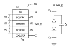
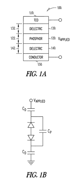
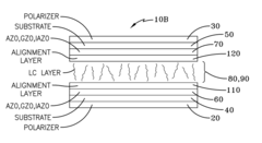
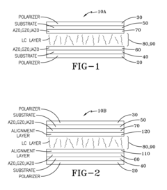
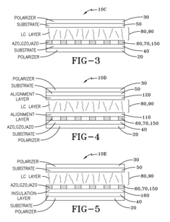
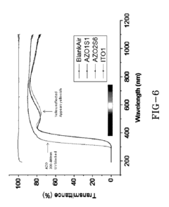
- The use of aluminum zinc oxide (AZO), gallium zinc oxide (GZO), and indium composites such as indium aluminum zinc oxide (IAZO) as transparent conductive oxide electrodes in electro-optical devices, which are optimized for etching processes to form fine patterns, allowing for reduced indium concentration (1-15%) and enhanced material parameters like dielectric constant and carrier mobility.
Environmental Impact of TCO Manufacturing Processes
The manufacturing processes of Transparent Conductive Oxides (TCOs) present significant environmental challenges that require careful consideration in the development and deployment of optical devices. Traditional TCO production methods, particularly those involving indium tin oxide (ITO), consume substantial energy and generate considerable waste. The high-temperature vacuum deposition techniques commonly employed for ITO coating require temperatures exceeding 300°C, resulting in significant carbon emissions estimated at 15-20 kg CO2 per square meter of coated surface.
Chemical precursors used in TCO manufacturing pose additional environmental concerns. The extraction of indium, a critical component in ITO, involves environmentally damaging mining practices and generates toxic byproducts including heavy metals and acidic waste. Current global indium mining operations produce approximately 1.5 million tons of waste annually, with only about 15% of mined indium effectively recovered for industrial applications.
Water consumption represents another significant environmental impact factor. Conventional TCO manufacturing processes require substantial quantities of ultra-pure water for cleaning and processing, with estimates suggesting 200-300 liters of water consumption per square meter of TCO material produced. The resulting wastewater often contains metal ions and chemical residues requiring specialized treatment before discharge.
Recent life cycle assessment (LCA) studies comparing various TCO materials have revealed that alternative materials such as fluorine-doped tin oxide (FTO) and aluminum-doped zinc oxide (AZO) demonstrate 30-40% lower environmental impact scores compared to ITO across multiple categories including global warming potential, acidification, and resource depletion. These alternatives, while promising, still present their own environmental challenges related to production efficiency and durability.
Emerging green manufacturing techniques show potential for reducing environmental impacts. Solution-based deposition methods operating at lower temperatures (below 200°C) can reduce energy consumption by up to 60% compared to vacuum-based processes. Additionally, closed-loop recycling systems implemented by leading manufacturers have demonstrated recovery rates of up to 85% for indium and other valuable materials from production waste and end-of-life devices.
Regulatory frameworks worldwide are increasingly addressing TCO manufacturing impacts. The European Union's Restriction of Hazardous Substances (RoHS) directive and similar regulations in Asia and North America have established limits on toxic substances in electronic components, driving research toward more environmentally benign TCO alternatives and manufacturing processes. Industry certification programs like EPEAT now include criteria specifically addressing the environmental footprint of transparent conductors in display technologies.
Supply Chain Analysis for TCO Raw Materials
The global supply chain for Transparent Conductive Oxide (TCO) materials represents a complex network spanning multiple continents and involving various stakeholders. Primary raw materials for TCO production include indium, tin, zinc, and gallium, with indium being particularly critical for the widely used Indium Tin Oxide (ITO). Currently, China dominates the global indium production, accounting for approximately 55-60% of worldwide supply, followed by South Korea and Japan. This geographic concentration creates significant supply vulnerabilities for manufacturers of optical devices utilizing TCO materials.
The extraction and processing of these materials involve multiple stages, beginning with mining of primary ores (primarily zinc, as indium is typically a byproduct), followed by refining, purification, and target manufacturing. The supply chain exhibits notable bottlenecks at the refining stage, where specialized technical expertise and equipment are required to achieve the high purity levels necessary for optical applications.
Price volatility represents a major challenge in TCO raw material procurement. Indium prices have fluctuated significantly over the past decade, with variations exceeding 300% during peak periods. This volatility is driven by limited supply sources, changing demand patterns in display technologies, and geopolitical factors affecting major producing regions. Such price instability complicates long-term planning for optical device manufacturers and can significantly impact production costs.
Environmental and sustainability concerns are increasingly influencing TCO supply chains. Traditional extraction methods for indium and other TCO materials generate substantial waste and consume significant energy. Recent regulatory changes in major producing countries have imposed stricter environmental standards, potentially constraining supply while increasing production costs. Several leading optical device manufacturers have initiated responsible sourcing programs to address these concerns.
Alternative supply strategies are emerging to mitigate risks associated with traditional TCO material sourcing. These include development of recycling technologies to recover indium and other materials from end-of-life products, establishment of strategic reserves by major consuming nations, and formation of joint ventures between device manufacturers and material suppliers to ensure stable supply. Additionally, research into alternative TCO materials with more abundant constituent elements is gaining momentum, though commercial viability remains limited for most alternatives.
The COVID-19 pandemic exposed significant vulnerabilities in the TCO supply chain, with disruptions in mining operations and international shipping causing temporary shortages and price spikes. This experience has accelerated efforts toward supply chain diversification and localization of certain processing capabilities in major consuming regions, particularly in North America and Europe.
Unlock deeper insights with Patsnap Eureka Quick Research — get a full tech report to explore trends and direct your research. Try now!
Generate Your Research Report Instantly with AI Agent
Supercharge your innovation with Patsnap Eureka AI Agent Platform!
