Research on Transparent Conductive Oxides in Photovoltaics
OCT 27, 20259 MIN READ
Generate Your Research Report Instantly with AI Agent
Patsnap Eureka helps you evaluate technical feasibility & market potential.
TCO Evolution and Research Objectives
Transparent Conductive Oxides (TCOs) have evolved significantly since their initial discovery in the early 20th century. The journey began with the development of tin-doped indium oxide (ITO) in the 1940s, which revolutionized transparent electronics. By the 1970s, TCOs had found their way into photovoltaic applications, marking a critical milestone in solar cell technology. The evolution accelerated in the 1990s with the emergence of alternative TCO materials such as fluorine-doped tin oxide (FTO) and aluminum-doped zinc oxide (AZO), addressing the scarcity and cost concerns associated with indium.
The technological progression of TCOs in photovoltaics has been driven by the increasing demands for higher efficiency, lower cost, and environmental sustainability. Early TCO implementations focused primarily on transparency and conductivity, while modern research emphasizes additional properties including work function tunability, chemical stability, and mechanical flexibility. This multifaceted approach has expanded the application scope of TCOs beyond traditional silicon-based solar cells to emerging technologies such as perovskite solar cells and organic photovoltaics.
Current research objectives in TCO development for photovoltaics center around several key areas. First, enhancing the figure of merit (FOM) which balances optical transparency with electrical conductivity – a fundamental trade-off in TCO materials. Second, developing indium-free alternatives to address the sustainability concerns of ITO, which remains the industry standard despite indium's limited supply. Third, improving the interface properties between TCOs and adjacent layers in solar cell architectures to minimize recombination losses and enhance charge extraction.
Another critical research direction involves the development of TCOs compatible with flexible substrates to enable roll-to-roll manufacturing processes and building-integrated photovoltaics. This requires TCO materials and deposition methods that can withstand mechanical stress without compromising electrical and optical properties. Additionally, researchers are exploring nanostructured TCOs to enhance light trapping and reduce reflection losses, potentially increasing the overall efficiency of solar devices.
The ultimate objective of TCO research in photovoltaics is to develop materials that can be manufactured at scale with consistent properties, minimal environmental impact, and competitive costs. This involves not only material innovation but also process optimization to ensure compatibility with existing manufacturing infrastructure. As photovoltaic technology continues to diversify beyond traditional silicon, TCO materials must evolve to meet the specific requirements of each solar cell architecture, creating a rich landscape for technological innovation and scientific discovery.
Market Analysis for TCO in Solar Applications
The global market for Transparent Conductive Oxides (TCOs) in photovoltaic applications has experienced significant growth over the past decade, driven by the expanding solar energy sector. The market value of TCOs specifically for solar applications reached approximately $2.5 billion in 2022, with projections indicating a compound annual growth rate (CAGR) of 12.3% through 2028.
Indium Tin Oxide (ITO) currently dominates the TCO market with over 60% market share due to its superior optical and electrical properties. However, concerns regarding indium scarcity and price volatility have accelerated the development of alternative materials. Fluorine-doped Tin Oxide (FTO) and Aluminum-doped Zinc Oxide (AZO) have emerged as the fastest-growing segments, with market shares of 22% and 15% respectively.
Regional analysis reveals Asia-Pacific as the dominant manufacturing hub for TCO materials, accounting for approximately 70% of global production. China leads manufacturing capacity, followed by South Korea and Japan. North America and Europe represent significant consumption markets, driven by government incentives for renewable energy adoption and strong research infrastructure.
The demand for TCOs in thin-film solar technologies is particularly robust, growing at 15.7% annually, outpacing the overall market. This is attributed to the increasing efficiency of thin-film technologies and their expanding applications in building-integrated photovoltaics (BIPV) and flexible solar panels.
Price sensitivity remains a critical factor in TCO market dynamics. The average cost of ITO has fluctuated between $600-800 per kilogram over the past five years, creating opportunities for more cost-effective alternatives. This has accelerated research into novel materials like graphene-based conductors and silver nanowires, though these remain in early commercialization stages.
Industry surveys indicate that solar manufacturers prioritize three key performance metrics when selecting TCO materials: optical transparency (>85%), sheet resistance (<10 ohms/square), and production cost. The balance of these factors varies by application, with high-efficiency solar cells demanding premium TCO materials despite higher costs.
Market forecasts suggest that next-generation TCOs with enhanced durability and reduced material costs could capture up to 30% of the market by 2030. This transition is expected to be particularly pronounced in emerging solar markets in Southeast Asia, Latin America, and Africa, where cost considerations often outweigh marginal efficiency gains.
Current TCO Technologies and Challenges
Transparent Conductive Oxides (TCOs) represent a critical component in photovoltaic technology, serving as essential materials for front electrodes in solar cells. Currently, the most widely deployed TCO materials include Indium Tin Oxide (ITO), Fluorine-doped Tin Oxide (FTO), and Aluminum-doped Zinc Oxide (AZO). ITO dominates the market due to its excellent combination of high transparency (>85% in visible spectrum) and low sheet resistance (<10 Ω/sq), making it ideal for high-efficiency solar applications.
Despite its superior performance, ITO faces significant challenges, primarily related to the scarcity and high cost of indium. Global indium reserves are limited, with prices fluctuating dramatically in recent years, creating supply chain vulnerabilities for photovoltaic manufacturers. This economic constraint has accelerated research into alternative TCO materials that can match ITO's performance while using more abundant elements.
FTO has emerged as a viable alternative in certain applications, particularly in dye-sensitized solar cells and perovskite photovoltaics. It offers better thermal stability than ITO and can withstand higher processing temperatures (up to 600°C compared to ITO's 350°C limit). However, FTO typically exhibits slightly higher sheet resistance and lower transparency, resulting in efficiency trade-offs in solar devices.
AZO represents another promising alternative, utilizing the abundant element zinc. While AZO demonstrates good optical and electrical properties, it suffers from stability issues, particularly in humid environments where performance degradation occurs rapidly. This limitation has restricted its widespread adoption in commercial photovoltaic applications despite its cost advantages.
Current manufacturing processes for TCOs also present significant challenges. Conventional deposition methods include magnetron sputtering, chemical vapor deposition, and sol-gel techniques. These processes often require high vacuum conditions or elevated temperatures, contributing substantially to the overall energy footprint and cost of solar cell production. The industry faces a pressing need for low-temperature, atmospheric pressure deposition techniques that can maintain material quality while reducing manufacturing costs.
Thickness uniformity and defect control remain persistent technical challenges across all TCO materials. Even minor variations in film thickness can lead to significant performance inconsistencies across large-area solar panels. Additionally, structural defects and grain boundaries in TCO films create recombination centers that reduce charge carrier mobility and overall device efficiency.
The development of flexible photovoltaics introduces additional requirements for TCO materials, as mechanical durability becomes crucial. Traditional TCOs often crack under bending stress, necessitating the development of novel compositions and nanostructured variants that can maintain conductivity under mechanical deformation while preserving optical transparency.
State-of-the-Art TCO Implementation Methods
01 Composition and structure of transparent conductive oxides
Transparent conductive oxides (TCOs) are materials that combine electrical conductivity with optical transparency. These materials typically consist of metal oxides doped with specific elements to enhance their conductivity while maintaining transparency. Common TCO compositions include indium tin oxide (ITO), zinc oxide (ZnO), and tin oxide (SnO2). The crystalline structure and composition significantly influence the electrical and optical properties of these materials, making them suitable for various optoelectronic applications.- Composition and structure of transparent conductive oxides: Transparent conductive oxides (TCOs) are materials that combine optical transparency with electrical conductivity. These materials typically consist of metal oxides doped with specific elements to enhance their conductivity while maintaining transparency. Common TCO compositions include indium tin oxide (ITO), zinc oxide (ZnO), and tin oxide (SnO2). The crystalline structure and composition significantly influence the electrical and optical properties of these materials, making them suitable for various electronic applications.
- Deposition methods for transparent conductive oxide films: Various deposition techniques are employed to create thin films of transparent conductive oxides on different substrates. These methods include sputtering, chemical vapor deposition (CVD), pulsed laser deposition, and sol-gel processes. Each technique offers distinct advantages in terms of film quality, uniformity, and production efficiency. The deposition parameters, such as temperature, pressure, and gas flow rates, significantly affect the resulting film properties, including transparency, conductivity, and adhesion to the substrate.
- Applications of transparent conductive oxides in electronic devices: Transparent conductive oxides are widely used in various electronic and optoelectronic devices. They serve as transparent electrodes in displays, touchscreens, solar cells, and light-emitting diodes (LEDs). In these applications, TCOs provide the necessary electrical conductivity while allowing light to pass through, enabling the functionality of these devices. The specific requirements for TCO properties vary depending on the application, with some requiring higher transparency while others prioritizing conductivity or flexibility.
- Enhancement of transparent conductive oxide properties: Various methods are employed to enhance the properties of transparent conductive oxides, including doping, annealing, and multilayer structures. Doping involves introducing specific elements into the oxide matrix to increase carrier concentration and improve conductivity. Annealing treatments can optimize the crystalline structure and reduce defects, leading to better performance. Additionally, creating multilayer structures or composites with other materials can result in TCOs with improved stability, flexibility, or specific optical characteristics tailored for particular applications.
- Novel transparent conductive oxide materials and fabrication techniques: Research in transparent conductive oxides focuses on developing new materials and innovative fabrication techniques to overcome limitations of traditional TCOs. This includes exploring alternative compositions such as aluminum-doped zinc oxide (AZO), fluorine-doped tin oxide (FTO), and various ternary compounds. Novel processing methods, such as solution-based approaches, atomic layer deposition, and nanostructuring, are being investigated to create TCOs with enhanced properties, reduced costs, or decreased environmental impact. These advancements aim to address challenges like indium scarcity, flexibility requirements, and performance in extreme conditions.
02 Fabrication methods for transparent conductive oxide films
Various deposition techniques are employed to fabricate transparent conductive oxide films with controlled properties. These methods include sputtering, chemical vapor deposition, sol-gel processing, and atomic layer deposition. The processing parameters such as temperature, pressure, and gas composition during deposition significantly affect the film quality, crystallinity, and performance characteristics. Post-deposition treatments like annealing can further enhance the electrical conductivity and optical transparency of these films.Expand Specific Solutions03 Applications in display and touch screen technologies
Transparent conductive oxides are widely used in display and touch screen technologies due to their unique combination of electrical conductivity and optical transparency. These materials serve as transparent electrodes in liquid crystal displays (LCDs), organic light-emitting diodes (OLEDs), and capacitive touch panels. The performance requirements include high visible light transmission, low sheet resistance, good adhesion to substrates, and mechanical durability under repeated touch operations.Expand Specific Solutions04 Transparent conductive oxides for photovoltaic applications
In photovoltaic devices, transparent conductive oxides function as front electrodes that allow light to pass through while collecting generated charge carriers. These materials are critical components in thin-film solar cells, perovskite solar cells, and other next-generation photovoltaic technologies. The development focuses on achieving optimal balance between transparency in the solar spectrum range and electrical conductivity, while also considering factors such as work function matching with adjacent layers and long-term stability under solar radiation.Expand Specific Solutions05 Novel transparent conductive oxide materials and composites
Research on novel transparent conductive oxide materials aims to overcome limitations of traditional TCOs such as indium scarcity and brittleness. This includes development of indium-free alternatives, composite structures, and nanostructured TCOs with enhanced properties. Approaches include doping conventional oxides with alternative elements, creating multilayer structures, incorporating nanomaterials like carbon nanotubes or graphene, and developing solution-processable TCO formulations. These innovations target improved conductivity-transparency trade-off, flexibility, and cost-effectiveness for next-generation electronic devices.Expand Specific Solutions
Leading Companies and Research Institutions
The transparent conductive oxide (TCO) market in photovoltaics is currently in a growth phase, with increasing demand driven by the expanding solar energy sector. The global market size is projected to reach significant value as solar installations continue to rise worldwide. Technologically, TCOs are advancing from traditional materials toward higher efficiency and lower-cost alternatives. Leading companies demonstrate varying levels of technological maturity: First Solar has achieved commercial success with CdTe technology, while research institutions like ICFO and CNRS are developing next-generation TCOs. Ubiquitous Energy represents innovation with transparent solar technology, while established manufacturers like AGC and Applied Materials provide industrial scale solutions. Companies such as Samsung Electronics and Trina Solar are integrating advanced TCOs into mainstream photovoltaic products, indicating the technology's transition toward broader commercial adoption.
First Solar, Inc.
Technical Solution: First Solar has developed proprietary cadmium telluride (CdTe) thin-film photovoltaic technology that incorporates specialized transparent conductive oxide layers. Their approach uses a unique high-resistance transparent (HRT) buffer layer combined with traditional TCO materials to enhance device performance. First Solar's manufacturing process employs a modified close-spaced sublimation technique for TCO deposition that achieves high throughput while maintaining precise control over film properties[2]. Their TCO stack typically consists of a tin oxide base layer with carefully controlled doping profiles to achieve sheet resistances of approximately 8-15 ohms/square while maintaining over 80% optical transmission in relevant wavelength ranges[4]. First Solar has also pioneered the use of magnesium-doped zinc oxide as an alternative TCO material that provides improved stability and reduced optical losses at interfaces. Their recent research has focused on TCO materials that can withstand their proprietary high-temperature CdTe deposition process while maintaining electrical and optical performance, resulting in modules with conversion efficiencies exceeding 19% in commercial production[5].
Strengths: Highly optimized TCO solutions specifically designed for CdTe technology with proven durability in field conditions. Their vertically integrated manufacturing approach allows for tight quality control and continuous improvement of TCO properties. Weaknesses: Their TCO technology is highly specialized for CdTe applications and may not be directly transferable to other photovoltaic technologies. The use of cadmium in their overall technology raises some environmental concerns despite their comprehensive recycling program.
Applied Materials, Inc.
Technical Solution: Applied Materials has developed advanced deposition technologies for transparent conductive oxides (TCOs) in photovoltaic applications, focusing on high-volume manufacturing solutions. Their primary approach involves physical vapor deposition (PVD) and chemical vapor deposition (CVD) systems that enable precise control over TCO film properties. Their flagship AKT-PX PECVD system allows for uniform deposition of indium tin oxide (ITO), aluminum-doped zinc oxide (AZO), and fluorine-doped tin oxide (FTO) films with thickness variations below 2% across large substrates[1]. Applied Materials has also pioneered the integration of TCO deposition with in-line quality monitoring systems that use optical and electrical measurements to ensure consistent performance metrics such as sheet resistance (typically achieving <10 ohms/square) and optical transparency (>85% in the visible spectrum)[3]. Their recent innovations include multi-layer TCO stacks that combine different materials to optimize both conductivity and transparency while reducing indium usage by up to 40%.
Strengths: Industry-leading equipment for high-volume, uniform TCO deposition with excellent process control and repeatability. Their integrated manufacturing approach enables seamless integration into existing production lines. Weaknesses: Their solutions typically require significant capital investment, making them less accessible to smaller manufacturers. Some of their TCO formulations still rely heavily on indium, which faces supply constraints and price volatility.
Key Patents and Scientific Breakthroughs
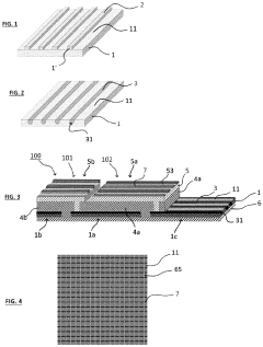
Transparent electrically conductive layer and method for forming same
PatentInactiveAU2011202985A1
Innovation
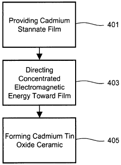
- A method involving the use of concentrated electromagnetic energy, specifically from a laser, to locally heat and crystallize cadmium-tin oxide ceramic layers, eliminating the need for vacuum annealing and enhancing conductivity and transparency.
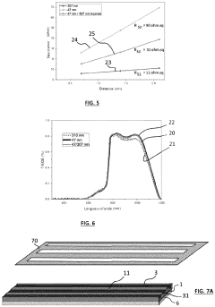
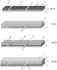
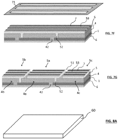
Photovoltaic cell provided with at least one improved conductive transparent oxide layer
PatentPendingEP4177967A1
Innovation
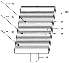
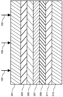
- A photovoltaic cell design featuring alternating bands of higher and lower resistivity in transparent conductive oxide layers, such as tin-doped indium oxide (ITO), zinc-doped indium oxide (IZO), or zinc-doped aluminum oxide (AZO), with localized overdoping to increase conductivity without increasing thickness, allowing for improved transparency and conductivity ratios.
Environmental Impact and Sustainability
The environmental impact of Transparent Conductive Oxides (TCOs) in photovoltaic applications represents a critical consideration in the sustainable development of solar energy technologies. TCOs, primarily composed of materials such as indium tin oxide (ITO), fluorine-doped tin oxide (FTO), and aluminum-doped zinc oxide (AZO), present both environmental challenges and opportunities throughout their lifecycle.
Manufacturing processes for TCOs often involve energy-intensive methods including sputtering, chemical vapor deposition, and sol-gel techniques. These processes contribute significantly to the carbon footprint of photovoltaic devices. Particularly concerning is the extraction of rare elements like indium, which faces supply constraints and requires environmentally disruptive mining operations. The scarcity of indium has prompted research into alternative TCO materials with reduced environmental impact.
Toxicity concerns also arise with certain TCO components. For instance, the potential leaching of heavy metals from damaged or improperly disposed solar panels presents environmental risks. This has led to increased focus on developing non-toxic alternatives and establishing robust recycling protocols for end-of-life photovoltaic systems incorporating TCOs.
Energy payback time (EPBT) represents another crucial metric for assessing TCO sustainability in photovoltaics. Recent advancements have reduced the EPBT for TCO-based solar cells, with modern technologies achieving payback periods of 1-2 years in optimal conditions. This improvement significantly enhances the net environmental benefit of photovoltaic systems over their operational lifetime.
Recycling and circular economy approaches are gaining prominence in TCO research. Novel methods for recovering valuable materials from decommissioned solar panels show promise for reducing primary resource demand. Hydrometallurgical and pyrometallurgical processes have demonstrated effective recovery rates for indium and other critical elements from TCO layers, though commercial-scale implementation remains limited.
Emerging research focuses on developing bio-based and environmentally benign TCO alternatives. Materials derived from sustainable sources, including cellulose-based composites and carbon-based nanomaterials, represent promising directions for reducing environmental impact while maintaining necessary optical and electrical properties for photovoltaic applications.
Life Cycle Assessment (LCA) studies indicate that despite manufacturing-related environmental costs, TCO-based photovoltaic systems deliver substantial net environmental benefits through clean energy generation. Continued improvements in manufacturing efficiency, material utilization, and end-of-life management will further enhance the sustainability profile of TCOs in photovoltaic applications.
Manufacturing Scalability and Cost Analysis
The scalability of Transparent Conductive Oxide (TCO) manufacturing processes represents a critical factor in the widespread adoption of advanced photovoltaic technologies. Current industrial production methods for TCOs include magnetron sputtering, chemical vapor deposition (CVD), and sol-gel processes, each with distinct cost implications and production capacities. Magnetron sputtering dominates commercial production due to its reliability and film quality consistency, though it requires significant capital investment with typical equipment costs ranging from $500,000 to several million dollars.
Production throughput analysis indicates that roll-to-roll manufacturing processes can achieve deposition rates of 10-50 nm/min over large areas, significantly reducing per-unit costs compared to batch processing methods. Recent advancements in high-power impulse magnetron sputtering (HiPIMS) have demonstrated 30% improvement in deposition efficiency while maintaining optical and electrical properties, potentially reducing production costs by 15-20% compared to conventional DC sputtering.
Material cost considerations reveal substantial differences between TCO options. Indium tin oxide (ITO) remains the industry standard despite raw material costs of approximately $600-800/kg for indium, while alternative materials like fluorine-doped tin oxide (FTO) and aluminum-doped zinc oxide (AZO) offer material cost reductions of 60-70% but with performance trade-offs in conductivity or transparency.
Energy consumption metrics indicate that TCO deposition processes typically require 5-15 kWh/m² of coated surface, representing 8-12% of the total energy input for photovoltaic module manufacturing. Implementation of energy recovery systems and process optimization has demonstrated potential energy savings of 20-25% in advanced production facilities.
Yield analysis across manufacturing scales shows defect rates decreasing from 15-20% in pilot production to 3-5% in fully optimized high-volume manufacturing lines. This improvement significantly impacts overall cost structures, with each percentage point of yield improvement translating to approximately 0.7-1.0% reduction in final module cost.
Economic modeling suggests that TCO materials and deposition processes currently contribute $0.03-0.07/watt to overall photovoltaic module costs. Sensitivity analysis indicates that achieving manufacturing scale of >100 MW annual production capacity represents a critical threshold for cost competitiveness, with economies of scale reducing TCO-related costs by up to 40% compared to smaller production volumes.
Unlock deeper insights with Patsnap Eureka Quick Research — get a full tech report to explore trends and direct your research. Try now!
Generate Your Research Report Instantly with AI Agent
Supercharge your innovation with Patsnap Eureka AI Agent Platform!