

How Transparent Conductive Oxides Optimize Material Properties
OCT 27, 20259 MIN READ
Generate Your Research Report Instantly with AI Agent
Patsnap Eureka helps you evaluate technical feasibility & market potential.
TCO Development History and Objectives
Transparent Conductive Oxides (TCOs) emerged in the early 20th century with the discovery of cadmium oxide's unique properties in 1907. However, significant development began in the 1940s when tin-doped indium oxide (ITO) was first reported. The 1970s marked a pivotal era as the semiconductor industry's growth created substantial demand for materials combining optical transparency with electrical conductivity. This period saw the first commercial applications of TCOs in liquid crystal displays and solar cells, establishing their fundamental role in optoelectronic devices.
The evolution of TCOs has been driven by the continuous optimization of three critical properties: optical transparency, electrical conductivity, and processability. Early research focused primarily on achieving acceptable levels of transparency and conductivity, often sacrificing one for the other. The 1980s and 1990s witnessed significant advancements in deposition techniques, particularly magnetron sputtering and chemical vapor deposition, enabling more precise control over material composition and structure.
By the early 2000s, the electronics industry's rapid expansion created new challenges for TCO development. The increasing scarcity and cost of indium prompted intensive research into alternative materials, including zinc oxide (ZnO), fluorine-doped tin oxide (FTO), and aluminum-doped zinc oxide (AZO). This diversification reflected a broader objective: developing TCOs with comparable performance to ITO but using more abundant and cost-effective elements.
The current technological landscape has further expanded TCO objectives to include flexibility, durability, and environmental sustainability. Modern applications in flexible electronics, touchscreens, and next-generation solar cells demand TCOs that maintain performance under mechanical stress and environmental exposure. Additionally, the push toward green technology has prioritized reducing toxic elements and energy-intensive processing in TCO production.
Looking forward, TCO development aims to achieve multifunctional capabilities beyond traditional conductivity and transparency. Research is increasingly focused on TCOs with tunable work functions, enhanced carrier mobility, and compatibility with emerging manufacturing techniques like roll-to-roll processing and 3D printing. The ultimate goal is to develop TCOs that can be tailored for specific applications while maintaining optimal performance across all critical parameters.
The trajectory of TCO development reflects a continuous refinement process, moving from simple binary oxides to complex multi-component systems with precisely engineered defect structures and interfaces. This evolution underscores the technology's responsiveness to changing market demands and its critical role in enabling advances across multiple industries, from consumer electronics to renewable energy and beyond.
Market Applications and Demand Analysis
The transparent conductive oxide (TCO) market has experienced significant growth driven by the expanding electronics industry, particularly in display technologies. The global TCO market was valued at approximately 7 billion USD in 2022 and is projected to grow at a compound annual growth rate of 6.8% through 2030. This growth is primarily fueled by increasing demand for touchscreen devices, flat panel displays, photovoltaic cells, and smart windows, all of which require materials with both optical transparency and electrical conductivity.
The display industry represents the largest application segment for TCOs, accounting for over 40% of market demand. Indium tin oxide (ITO) continues to dominate this sector due to its excellent combination of transparency (>90% in visible spectrum) and conductivity (resistivity as low as 10^-4 Ω·cm). However, the limited availability and rising cost of indium have prompted manufacturers to seek alternative TCO materials, creating new market opportunities for materials like fluorine-doped tin oxide (FTO), aluminum-doped zinc oxide (AZO), and gallium-doped zinc oxide (GZO).
The photovoltaic industry has emerged as the fastest-growing application segment for TCOs, with an annual growth rate exceeding 12%. This surge is driven by global renewable energy initiatives and the critical role TCOs play in solar cell efficiency. TCOs serve as transparent electrodes in thin-film solar cells, where optimization of carrier concentration (typically 10^20-10^21 cm^-3) and mobility (>40 cm²/Vs) directly impacts energy conversion efficiency.
Regionally, Asia-Pacific dominates the TCO market with approximately 65% share, led by manufacturing powerhouses in China, South Korea, Japan, and Taiwan. North America and Europe follow with significant market shares driven by advanced research and development activities focused on next-generation TCO materials with enhanced properties.
The automotive sector represents an emerging application area with substantial growth potential. The integration of smart glass technologies, heads-up displays, and photovoltaic sunroofs in modern vehicles is creating new demand for TCOs with specialized properties such as enhanced durability, flexibility, and temperature stability. Industry analysts project this segment to grow at 9.5% annually through 2030.
Material optimization trends in the TCO market are increasingly focused on achieving specific property combinations tailored to application requirements. For display technologies, the focus is on balancing high transparency (>85%) with low sheet resistance (<10 Ω/sq) and mechanical flexibility. For photovoltaic applications, the emphasis is on wide bandgap (>3.0 eV), high carrier mobility, and long-term environmental stability. These application-specific requirements are driving specialized research and development efforts across the TCO value chain.
Current TCO Materials and Technical Challenges
Transparent Conductive Oxides (TCOs) represent a critical class of materials in modern optoelectronic applications, with Indium Tin Oxide (ITO) dominating the commercial market due to its excellent combination of optical transparency and electrical conductivity. ITO typically achieves transmittance above 85% in the visible spectrum while maintaining sheet resistances below 100 Ω/sq. However, the scarcity and rising cost of indium have driven extensive research into alternative TCO materials.
Fluorine-doped Tin Oxide (FTO) has emerged as a cost-effective alternative with superior thermal stability compared to ITO, making it particularly suitable for solar cell applications. Aluminum-doped Zinc Oxide (AZO) offers another promising option with abundant constituent elements, though it suffers from moisture sensitivity that limits its application in certain environments.
The fundamental technical challenge in TCO development stems from the inherent trade-off between optical transparency and electrical conductivity. These properties are intrinsically coupled through the carrier concentration - increasing carrier density improves conductivity but typically reduces transparency due to increased free carrier absorption. This relationship creates a performance ceiling that conventional doping strategies struggle to overcome.
Material stability presents another significant challenge, particularly for zinc-based TCOs which exhibit degradation under humid conditions. Mechanical flexibility limitations also restrict TCO application in emerging flexible electronics, as most oxide materials are inherently brittle and develop microcracks under bending stress, leading to conductivity losses.
Manufacturing scalability remains problematic for many promising TCO candidates. While ITO benefits from well-established industrial processes, alternatives often require specialized deposition techniques that are difficult to scale economically. The industry faces significant challenges in transitioning from laboratory demonstrations to cost-effective mass production.
Environmental concerns have also emerged as a critical consideration, with regulations increasingly restricting the use of toxic elements in electronic materials. This has accelerated research into environmentally benign TCO compositions that maintain performance standards while eliminating hazardous components.
Recent advances in computational materials science have enabled more systematic exploration of the TCO composition space, identifying promising dopant combinations and predicting their properties. However, translating these theoretical insights into practical materials often reveals unforeseen challenges in synthesis and processing that require extensive experimental optimization.
The geographical distribution of TCO research and production capabilities shows significant concentration in East Asia, particularly Japan, South Korea, and China, where display manufacturing is centered. This regional specialization has implications for supply chain resilience and technology transfer in the global TCO ecosystem.
Current Optimization Methods for TCO Properties
01 Composition and structure of transparent conductive oxides
Transparent conductive oxides (TCOs) are materials that combine electrical conductivity with optical transparency. Common TCO materials include indium tin oxide (ITO), zinc oxide (ZnO), and tin oxide (SnO2). These materials can be doped with various elements to enhance their electrical and optical properties. The crystalline structure and composition significantly influence the performance of TCOs, with factors such as oxygen vacancies and dopant concentration playing crucial roles in determining conductivity while maintaining transparency.- Composition and structure of transparent conductive oxides: Transparent conductive oxides (TCOs) are materials that combine electrical conductivity with optical transparency. Common TCO materials include indium tin oxide (ITO), zinc oxide (ZnO), and tin oxide (SnO2). These materials can be doped with various elements to enhance their electrical and optical properties. The crystalline structure and composition of TCOs significantly influence their performance characteristics, including transparency, conductivity, and stability.
- Deposition and fabrication methods for TCO films: Various deposition techniques are employed to fabricate transparent conductive oxide films, including sputtering, chemical vapor deposition (CVD), sol-gel methods, and pulsed laser deposition. The deposition parameters such as temperature, pressure, and gas flow rate significantly affect the resulting film properties. Post-deposition treatments like annealing can further enhance the electrical conductivity and optical transparency of TCO films by improving crystallinity and reducing defects.
- Electrical and optical properties of TCO materials: Transparent conductive oxides exhibit unique electrical and optical properties that make them valuable for various applications. These materials typically have a wide bandgap (>3 eV) that allows visible light transmission while maintaining electrical conductivity. Key properties include sheet resistance, carrier concentration, mobility, work function, and optical transmittance. The balance between conductivity and transparency can be tuned through composition control and processing conditions to meet specific application requirements.
- TCO applications in electronic and optoelectronic devices: Transparent conductive oxides are widely used in various electronic and optoelectronic devices. They serve as transparent electrodes in displays, touchscreens, solar cells, and light-emitting diodes. TCOs are also employed in smart windows, electromagnetic shielding, and gas sensors. The specific material properties required vary by application, with some devices prioritizing conductivity while others require maximum transparency or specific work function values.
- Novel TCO materials and enhancement strategies: Research continues to develop novel transparent conductive oxide materials with improved properties. This includes exploring alternative compositions to reduce reliance on scarce elements like indium, developing nanostructured TCOs, and creating composite or multilayer structures. Enhancement strategies include co-doping, interface engineering, and incorporating other materials like graphene or metal nanowires. These approaches aim to overcome traditional trade-offs between transparency and conductivity while improving stability, flexibility, and cost-effectiveness.
02 Deposition methods and their effects on TCO properties
Various deposition techniques are used to fabricate transparent conductive oxide films, including sputtering, chemical vapor deposition, sol-gel processing, and pulsed laser deposition. The choice of deposition method significantly affects the material properties of the resulting TCO films, including crystallinity, grain size, surface roughness, and defect concentration. Process parameters such as temperature, pressure, and gas composition during deposition can be optimized to achieve desired electrical conductivity and optical transparency characteristics.Expand Specific Solutions03 Electrical and optical properties of TCO materials
Transparent conductive oxides exhibit unique combinations of electrical conductivity and optical transparency. Key electrical properties include carrier concentration, mobility, and resistivity, while optical properties encompass transmittance, reflectance, and absorption across different wavelength ranges. The trade-off between conductivity and transparency is a fundamental challenge in TCO development, as increasing carrier concentration typically enhances conductivity but reduces transparency due to increased free carrier absorption. Band gap engineering and defect management are essential strategies for optimizing this balance.Expand Specific Solutions04 TCO applications in electronic and optoelectronic devices
Transparent conductive oxides are widely used in various electronic and optoelectronic applications including touch screens, flat panel displays, solar cells, and smart windows. The specific material properties required vary by application - solar cells demand high transparency in specific wavelength ranges and sufficient conductivity for charge collection, while display applications require uniform optical and electrical properties across large areas. TCO materials can be patterned and integrated with other device components to create functional electronic systems that benefit from their unique combination of properties.Expand Specific Solutions05 Novel TCO materials and enhancement strategies
Research on transparent conductive oxides focuses on developing new materials and strategies to enhance their properties. This includes exploring alternative TCO compositions such as multicomponent oxides, nanostructured TCOs, and composite materials. Doping strategies, including co-doping and gradient doping, are employed to optimize carrier concentration while minimizing optical losses. Surface treatments and interface engineering techniques are used to improve stability and compatibility with adjacent materials in device structures. These innovations aim to overcome limitations of traditional TCOs such as indium scarcity and brittleness.Expand Specific Solutions
Leading Manufacturers and Research Institutions
The transparent conductive oxides (TCO) market is currently in a growth phase, driven by increasing demand for touchscreens, displays, and photovoltaic applications. The global market is projected to expand significantly due to rising adoption in smart devices and renewable energy sectors. Technologically, TCOs are advancing from established materials like indium tin oxide toward more sustainable alternatives. Leading companies including Pilkington Group, AGC Inc., and Sumitomo Chemical are focusing on enhancing optical transparency while maintaining electrical conductivity. Academic institutions such as Trinity College Dublin and Northwestern University collaborate with industrial players like Micron Technology and OSRAM to develop next-generation TCOs with improved durability, flexibility, and cost-effectiveness. The competitive landscape features both established glass manufacturers and specialized electronics materials companies working to optimize TCO properties for emerging applications.
Sumitomo Chemical Co., Ltd.
Technical Solution: Sumitomo Chemical has pioneered innovative TCO materials focusing on sustainability and performance enhancement. Their SOLARNO™ series utilizes zinc-based TCOs (primarily AZO and GZO) as alternatives to indium-based materials, addressing resource scarcity concerns. Sumitomo's proprietary sol-gel deposition technique enables low-temperature processing (below 200°C), making their TCOs compatible with temperature-sensitive substrates including flexible polymers. Their recent breakthrough involves nanocomposite TCOs incorporating carbon nanomaterials (graphene and carbon nanotubes) into metal oxide matrices, achieving sheet resistance as low as 5 ohms/square while maintaining >88% optical transparency. These hybrid materials demonstrate superior mechanical flexibility, withstanding over 10,000 bending cycles with less than 5% change in electrical conductivity, making them ideal for next-generation flexible electronics and photovoltaics. Sumitomo has also developed self-healing TCO formulations that can recover conductivity after minor mechanical damage through low-temperature annealing processes.
Strengths: Industry-leading research in indium-free TCO alternatives; excellent compatibility with flexible substrates; innovative nanocomposite approaches that enhance both electrical and mechanical properties. Weaknesses: Higher initial production costs compared to conventional ITO; potential long-term stability issues with some nanocomposite formulations; more complex quality control requirements for hybrid materials.
Semiconductor Energy Laboratory Co., Ltd.
Technical Solution: Semiconductor Energy Laboratory (SEL) has developed cutting-edge TCO materials specifically optimized for thin-film transistor (TFT) applications. Their IGZO (indium gallium zinc oxide) technology represents a significant advancement in amorphous oxide semiconductor materials, achieving electron mobility exceeding 10 cm²/Vs while maintaining transparency above 90% in the visible spectrum. SEL's proprietary CAAC (c-axis aligned crystalline) structure for oxide semiconductors enables unprecedented stability against environmental stressors and electrical stress, with negligible threshold voltage shift even after 10,000 hours of continuous operation. Their recent innovations include dual-layer TCO structures with gradient doping profiles that optimize both channel interface properties and contact resistance, resulting in TFTs with on/off ratios exceeding 10⁹. SEL has also pioneered ultra-thin TCO deposition techniques compatible with roll-to-roll processing, enabling TCO layers as thin as 20nm while maintaining sheet resistance below 50 ohms/square, critical for flexible display applications.
Strengths: World-leading expertise in oxide semiconductor TFT technology; exceptional stability and reliability characteristics; advanced manufacturing techniques enabling ultra-thin, uniform films. Weaknesses: Higher material complexity requiring precise composition control; more sophisticated deposition equipment requirements; primarily optimized for display applications rather than broader TCO uses.
Key Patents and Breakthroughs in TCO Materials
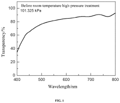
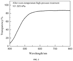
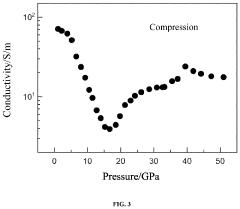
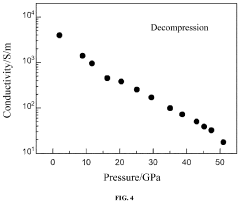
Method for improving conductivity and blue light filtering efficiency of transparent conducting oxide (TCO)
PatentActiveUS20240092650A1
Innovation
- A method involving room-temperature high-pressure treatment of indium oxide-based TCO materials, specifically titanium-doped indium oxide, which undergoes a structural phase transition from a cubic to a corundum structure, significantly enhancing conductivity and blue light filtering efficiency while maintaining high transparency.
Transparent conducting films including complex oxides
PatentActiveUS20160180982A1
Innovation
- Development of alkaline earth transition metal oxide films with specific chemical formulas, such as A1-xA′xB1-yB′yO3-d and (ABO3-d)m(A′B′O3-d′)n, which offer high carrier concentration, effective mass, and optical transparency through aliovalent substitution and laminated structures, enabling higher electrical conductivity and reduced optical absorption.
Environmental Impact and Sustainability Considerations
The production and deployment of transparent conductive oxides (TCOs) present significant environmental considerations that must be addressed for sustainable technological advancement. Manufacturing processes for TCOs often involve energy-intensive methods such as sputtering, chemical vapor deposition, and sol-gel techniques, which contribute substantially to carbon emissions. The optimization of these processes to reduce energy consumption represents a critical area for improvement in the industry's environmental footprint.
Material selection for TCOs also carries important sustainability implications. Traditional indium-based compounds like ITO (indium tin oxide) rely on indium, a scarce element with limited global reserves primarily concentrated in China, South Korea, and Japan. This scarcity has prompted research into alternative materials such as fluorine-doped tin oxide (FTO), aluminum-doped zinc oxide (AZO), and graphene-based composites that utilize more abundant elements.
Lifecycle assessment studies indicate that the environmental impact of TCOs extends beyond production to include disposal and recycling challenges. The complex composition of these materials often complicates end-of-life management, with potential for toxic element leaching if improperly handled. Advanced recycling technologies specifically designed for TCO recovery from electronic waste are emerging as essential components of a circular economy approach.
Water usage and chemical waste generation during TCO manufacturing present additional environmental concerns. Wet chemical processes employed in certain TCO production methods can generate significant volumes of wastewater containing metal ions and other contaminants. Implementation of closed-loop water systems and green chemistry principles can substantially mitigate these impacts.
Energy efficiency improvements in devices utilizing TCOs offer a positive environmental counterbalance. The enhanced performance of solar cells, smart windows, and energy-efficient displays enabled by optimized TCO materials contributes to reduced energy consumption throughout product lifespans. This beneficial effect must be quantified in comprehensive sustainability assessments of TCO technologies.
Regulatory frameworks worldwide are increasingly addressing the environmental aspects of electronic materials, including TCOs. The European Union's Restriction of Hazardous Substances (RoHS) directive and similar regulations in other regions impose limitations on toxic elements in electronic components. These evolving standards are driving innovation toward more environmentally benign TCO formulations and manufacturing processes.
Industry-academic collaborations focused on green TCO technologies demonstrate promising advances in sustainable material design. Bio-inspired approaches and ambient-temperature processing methods represent frontier research areas with potential to dramatically reduce the environmental footprint of next-generation transparent conductive materials.
Fabrication Techniques and Process Optimization
The fabrication of transparent conductive oxides (TCOs) represents a critical aspect in optimizing their material properties for various applications. Traditional deposition methods include magnetron sputtering, pulsed laser deposition (PLD), chemical vapor deposition (CVD), and sol-gel processes. Each technique offers distinct advantages in controlling film thickness, crystallinity, and electrical properties.
Magnetron sputtering has emerged as the industry standard for large-scale TCO production, particularly for indium tin oxide (ITO) films. This technique allows precise control over stoichiometry and produces highly uniform films with excellent adhesion. Recent advancements in high-power impulse magnetron sputtering (HiPIMS) have further enhanced the quality of TCO films by increasing ionization rates and improving film density without substrate heating.
Atomic layer deposition (ALD) represents a significant breakthrough in TCO fabrication, enabling atomic-level control over film growth. This technique produces exceptionally uniform and conformal coatings even on complex 3D structures. For zinc oxide-based TCOs, ALD has demonstrated superior control over dopant concentration and distribution, resulting in enhanced carrier mobility while maintaining optical transparency.
Post-deposition treatments significantly influence TCO performance characteristics. Thermal annealing in controlled atmospheres (vacuum, oxygen, hydrogen, or forming gas) can dramatically alter the electrical conductivity and optical properties. For instance, annealing ZnO:Al films at 400-500°C in hydrogen atmosphere reduces oxygen vacancies, increasing carrier concentration while maintaining high transparency in the visible spectrum.
Surface modification techniques, including plasma treatments and chemical functionalization, have proven effective in tailoring TCO work functions and interface properties. Oxygen plasma treatment of ITO surfaces can increase work function by up to 0.7 eV, critical for optimizing charge injection in optoelectronic devices. Conversely, reducing treatments can lower work functions to improve electron extraction in photovoltaic applications.
Recent innovations in solution-processed TCOs offer cost-effective alternatives to vacuum-based methods. Spray pyrolysis and inkjet printing of precursor solutions enable direct patterning capabilities without photolithography steps. These approaches have demonstrated particular promise for fluorine-doped tin oxide (FTO) and aluminum-doped zinc oxide (AZO) films, achieving resistivities approaching 10^-3 Ω·cm with optical transmittance exceeding 85%.
Roll-to-roll processing represents the frontier of TCO fabrication for flexible electronics. This continuous manufacturing approach combines atmospheric pressure spatial atomic layer deposition with rapid thermal processing, enabling high-throughput production of flexible TCO films on polymer substrates. Current research focuses on reducing processing temperatures while maintaining electrical performance to expand compatibility with temperature-sensitive substrate materials.
Unlock deeper insights with Patsnap Eureka Quick Research — get a full tech report to explore trends and direct your research. Try now!
Generate Your Research Report Instantly with AI Agent
Supercharge your innovation with Patsnap Eureka AI Agent Platform!