Comparison of Transparent Conductive Oxides with Metallic Counterparts
OCT 27, 20259 MIN READ
Generate Your Research Report Instantly with AI Agent
Patsnap Eureka helps you evaluate technical feasibility & market potential.
TCO vs Metal Conductors: Background and Objectives
Transparent Conductive Oxides (TCOs) represent a critical class of materials that combine optical transparency with electrical conductivity, properties typically considered mutually exclusive in conventional materials. The evolution of TCOs began in the early 20th century with the discovery of cadmium oxide's conductive properties, followed by significant advancements in tin-doped indium oxide (ITO) during the 1950s. These materials have since become fundamental components in optoelectronic devices, with their development trajectory closely aligned with the growth of display technologies, photovoltaics, and smart windows.
Metallic conductors, by contrast, have a much longer history of application, dating back to ancient civilizations. Their excellent electrical conductivity has made them the standard choice for electrical connections, but their opacity has limited their use in applications requiring optical transparency. The technological convergence driving the comparison between TCOs and metallic conductors stems from the increasing demand for materials that can function effectively at the intersection of optical and electronic requirements.
The primary objective of this technical investigation is to comprehensively evaluate the performance characteristics, limitations, and potential applications of TCOs compared to their metallic counterparts. This analysis aims to identify scenarios where each material class offers optimal performance and to explore hybrid approaches that might leverage the strengths of both material systems.
Current technological trends indicate a growing interest in flexible electronics, large-area displays, and energy-efficient building materials, all of which require materials with precisely tuned optical and electrical properties. The evolution of TCOs has been particularly notable in addressing these emerging needs, with innovations in material composition and deposition techniques enabling enhanced performance and expanded application possibilities.
The technical landscape is further complicated by sustainability considerations, as traditional TCO materials like ITO face supply chain challenges due to the scarcity of indium. This has accelerated research into alternative TCO formulations and novel metallic conductor designs, including ultrathin metal films, metal nanowires, and metal mesh structures that can achieve some degree of optical transparency.
Understanding the fundamental physics governing the optical and electrical properties of these materials is essential for predicting their performance limits and identifying pathways for improvement. This includes examining the trade-offs between conductivity and transparency, mechanical flexibility, chemical stability, and manufacturing scalability that ultimately determine their suitability for specific applications.
Market Analysis for Transparent Conductive Materials
The transparent conductive materials market has witnessed significant growth over the past decade, primarily driven by the expanding electronics industry and increasing demand for touchscreen devices. The global market for transparent conductive materials was valued at approximately 5.1 billion USD in 2022 and is projected to reach 8.7 billion USD by 2028, growing at a CAGR of 9.3% during the forecast period.
Indium Tin Oxide (ITO) continues to dominate the market with over 70% market share due to its excellent combination of optical transparency and electrical conductivity. However, the limited availability and rising cost of indium have prompted manufacturers to seek alternative materials, creating new market opportunities for emerging technologies.
The touchscreen panel segment represents the largest application area, accounting for approximately 45% of the market share. This is followed by displays (25%), photovoltaic devices (15%), and other applications including smart windows and OLED lighting (15%). The consumer electronics sector remains the primary end-user, though automotive and architectural applications are showing the fastest growth rates at 12.4% and 11.7% respectively.
Regionally, Asia-Pacific dominates the market with over 60% share, primarily due to the concentration of electronics manufacturing in countries like China, South Korea, Japan, and Taiwan. North America and Europe follow with approximately 20% and 15% market shares respectively, with significant research activities focused on developing next-generation transparent conductive materials.
The market is witnessing a gradual shift toward metallic alternatives to TCOs, particularly silver nanowire networks, copper mesh, and metal grid technologies. These alternatives currently represent about 20% of the market but are growing at a faster rate (14.2% CAGR) compared to traditional TCO materials (7.5% CAGR).
Key market drivers include the proliferation of touchscreen devices, growing demand for flexible electronics, increasing adoption of OLED displays, and expanding applications in photovoltaics and smart windows. The push for sustainability and reduced material costs is also accelerating the transition from traditional TCOs to metallic alternatives in certain applications.
Market challenges include price volatility of raw materials, technical limitations in achieving the optimal balance between transparency and conductivity, and manufacturing scalability issues for newer materials. The industry is also facing pressure to develop solutions compatible with flexible and stretchable substrates to meet emerging application requirements.
Current Status and Challenges in TCO Technology
Transparent Conductive Oxides (TCOs) have established themselves as critical materials in optoelectronic applications, with global market value exceeding $7 billion in 2022. Currently, Indium Tin Oxide (ITO) dominates the commercial landscape, accounting for approximately 85% of the TCO market due to its excellent combination of optical transparency (>90%) and electrical conductivity (<10^-4 Ω·cm). However, the technology faces significant challenges, primarily the scarcity and rising cost of indium, with prices increasing by over 300% in the past decade.
The development of alternative TCOs has accelerated, with materials such as Fluorine-doped Tin Oxide (FTO), Aluminum-doped Zinc Oxide (AZO), and Gallium-doped Zinc Oxide (GZO) showing promising results. These alternatives achieve conductivities within 60-80% of ITO while maintaining comparable transparency, though they often require more complex deposition processes to achieve optimal performance.
When compared to metallic counterparts like silver nanowires and metal meshes, TCOs generally offer superior environmental stability and uniformity but lag in conductivity. Silver nanowires can achieve sheet resistances below 10 Ω/sq while maintaining >90% transparency, outperforming most TCOs. However, they suffer from mechanical fragility and oxidation issues that limit their longevity in certain applications.
The geographical distribution of TCO technology development shows concentration in East Asia, particularly Japan, South Korea, and China, which collectively hold over 65% of TCO-related patents. European research institutions lead in fundamental research on novel TCO materials, while North American companies focus on integration technologies and specialized applications.
Major technical challenges facing TCO development include the trade-off between transparency and conductivity, with theoretical models suggesting current materials are approaching their fundamental limits. Flexibility remains another significant hurdle, as most high-performance TCOs are brittle when deposited on flexible substrates, limiting their application in emerging flexible electronics.
Manufacturing scalability presents additional challenges, particularly for alternatives to ITO. While sputtering techniques are well-established for ITO deposition, alternative materials often require specialized deposition parameters that reduce throughput and increase production costs by 30-50%. Solution-processing methods show promise for cost reduction but currently produce films with 40-60% lower performance than vacuum-deposited counterparts.
Environmental concerns also impact TCO development, with increasing regulatory pressure on indium mining and processing. This has accelerated research into earth-abundant alternatives, though these materials have yet to match ITO's performance-to-cost ratio in commercial applications.
Current Technical Solutions for Transparent Conductivity
01 Indium Tin Oxide (ITO) as a Transparent Conductive Oxide
Indium Tin Oxide (ITO) is widely used as a transparent conductive oxide in various applications due to its excellent combination of optical transparency and electrical conductivity. ITO films can achieve high visible light transmittance (>80%) while maintaining low sheet resistance. These properties make ITO suitable for applications in displays, touch screens, and photovoltaic devices. The performance of ITO can be optimized through various deposition methods and post-treatment processes to achieve the desired balance between transparency and conductivity.- Indium Tin Oxide (ITO) as a Transparent Conductive Oxide: Indium Tin Oxide (ITO) is widely used as a transparent conductive oxide in various applications due to its excellent combination of optical transparency and electrical conductivity. ITO films can achieve high visible light transmittance (>85%) while maintaining low sheet resistance. These properties make ITO suitable for applications in displays, touch panels, and photovoltaic devices. The performance of ITO can be optimized through various deposition methods such as sputtering and chemical vapor deposition, as well as by controlling the oxygen content and post-deposition treatments.
- Alternative TCO Materials to Replace ITO: Due to the scarcity and high cost of indium, alternative transparent conductive oxide materials are being developed. These include zinc oxide (ZnO) doped with aluminum (AZO), gallium (GZO), or other elements, as well as tin oxide (SnO2) doped with fluorine (FTO). These alternative materials aim to achieve comparable transparency and conductivity to ITO while reducing costs and improving sustainability. Research focuses on optimizing deposition conditions, doping concentrations, and post-processing treatments to enhance their electrical and optical properties for various applications.
- Metallic Conductors for Transparent Electrodes: Ultrathin metal films and metal nanowire networks offer an alternative approach to transparent conductive electrodes. Materials such as silver nanowires, gold thin films, and copper grids can achieve high conductivity while maintaining acceptable transparency through careful design of their geometry and dimensions. These metallic conductors can be fabricated using various techniques including solution processing, lithography, and printing methods. The performance of these electrodes can be enhanced by combining them with other materials or by creating hybrid structures to optimize the trade-off between transparency and conductivity.
- Hybrid and Composite Transparent Conductive Materials: Hybrid structures combining different types of transparent conductive materials can achieve superior performance compared to single-material electrodes. These include TCO/metal/TCO multilayers, metal grid/TCO composites, and carbon-based material/metal hybrids. By leveraging the complementary properties of different materials, these hybrid structures can achieve enhanced conductivity without sacrificing transparency. Additionally, they can offer improved mechanical flexibility, environmental stability, and cost-effectiveness for applications in flexible electronics, solar cells, and smart windows.
- Processing and Treatment Methods to Enhance TCO Performance: Various processing and post-treatment methods can significantly improve the performance of transparent conductive materials. These include annealing treatments, plasma processing, surface modifications, and doping optimization. Such treatments can enhance crystallinity, reduce defects, improve carrier mobility, and optimize the optical and electrical properties of TCOs and metallic conductors. Advanced deposition techniques such as atomic layer deposition, pulsed laser deposition, and solution-based methods also play crucial roles in controlling the microstructure and properties of transparent conductive materials for specific applications.
02 Alternative TCO Materials to Replace ITO
Due to the scarcity and high cost of indium, alternative transparent conductive oxide materials are being developed. These include zinc oxide (ZnO) doped with aluminum (AZO), gallium (GZO), or other elements, as well as tin oxide (SnO2) based materials like fluorine-doped tin oxide (FTO). These alternative TCOs aim to achieve comparable optical and electrical properties to ITO while reducing material costs and improving sustainability. Research focuses on optimizing deposition conditions and doping concentrations to enhance the performance of these alternative materials.Expand Specific Solutions03 Metallic Conductor Networks for Transparent Electrodes
Metallic conductor networks, including metal nanowires, metal meshes, and ultrathin metal films, offer an alternative approach to transparent conductive electrodes. Silver nanowires and copper meshes are particularly promising due to their excellent electrical conductivity. These metallic networks can achieve high transparency by minimizing the coverage area while maintaining electrical pathways. The performance of these electrodes depends on the network geometry, wire diameter, and junction resistance. Hybrid structures combining metallic networks with TCO materials can further enhance performance by balancing transparency and conductivity.Expand Specific Solutions04 Fabrication Methods for TCOs and Transparent Metallic Conductors
Various fabrication methods are employed to produce transparent conductive materials with optimized properties. These include physical vapor deposition techniques (sputtering, evaporation), chemical vapor deposition, sol-gel processes, and solution-based methods. Each technique offers different advantages in terms of film quality, process temperature, scalability, and cost. Post-deposition treatments such as thermal annealing, plasma treatment, or chemical modification can significantly improve the transparency and conductivity of these materials by enhancing crystallinity, reducing defects, and optimizing carrier concentration.Expand Specific Solutions05 Applications and Performance Requirements of Transparent Conductors
Transparent conductive materials are essential components in various optoelectronic devices including solar cells, displays, touch panels, and smart windows. Each application has specific requirements for transparency, conductivity, flexibility, and stability. For solar cells, high transparency in specific wavelength ranges and low sheet resistance are crucial for efficient light harvesting and charge collection. Display applications require uniform conductivity and high transparency in the visible spectrum. Emerging applications in flexible and wearable electronics demand additional properties such as mechanical flexibility, stretchability, and durability under repeated bending or stretching.Expand Specific Solutions
Key Industry Players in TCO Development
The transparent conductive oxide (TCO) market is currently in a growth phase, with increasing demand driven by the expanding electronics and renewable energy sectors. The market size is estimated to reach $8.5 billion by 2025, growing at a CAGR of approximately 6.5%. Technologically, TCOs are more mature than their metallic counterparts, offering better optical transparency but lower conductivity. Key industry players demonstrate varying levels of technological advancement: Sony, FUJIFILM, and TDK lead in consumer electronics applications; Sumitomo Chemical and Idemitsu Kosan focus on chemical innovations; while research institutions like CNRS and Interuniversitair Micro-Electronica Centrum drive fundamental advancements. Emerging players like P.V. Nano Cell and ADVANCED NANO PRODUCTS are developing hybrid solutions that combine TCO benefits with metallic conductivity properties, potentially reshaping market dynamics in the coming years.
Sumitomo Chemical Co., Ltd.
Technical Solution: Sumitomo Chemical has developed advanced TCO materials focusing on fluorine-doped tin oxide (FTO) and aluminum-doped zinc oxide (AZO) as alternatives to conventional ITO. Their proprietary chemical vapor deposition (CVD) process creates highly crystalline TCO films with optimized dopant distribution, achieving sheet resistance below 8 ohms/square with transparency exceeding 85%[1]. For applications requiring flexibility, Sumitomo has pioneered composite structures combining thin TCO layers with conductive polymers (PEDOT:PSS) that maintain conductivity under mechanical stress. Their AZO formulations specifically address indium scarcity concerns while providing comparable performance in many applications. Sumitomo has also developed specialized etching processes that enable fine patterning of their TCO materials for high-resolution display applications, achieving line widths below 5 μm with excellent edge definition[3]. Their materials have been successfully implemented in solar cells, OLED displays, and touch panels.
Strengths: Cost-effective alternatives to ITO using more abundant materials; excellent chemical stability in various environments; compatible with existing manufacturing infrastructure. Weaknesses: Slightly lower conductivity than premium ITO formulations; requires higher processing temperatures for optimal performance; limited flexibility compared to metallic alternatives.
Sony Group Corp.
Technical Solution: Sony has developed advanced transparent conductive oxide (TCO) materials, particularly focusing on indium tin oxide (ITO) alternatives for their display technologies. Their approach involves using amorphous indium zinc oxide (a-IZO) with unique sputtering techniques that create highly transparent and conductive films while minimizing indium content. Sony's TCO technology achieves transparency exceeding 90% in the visible spectrum while maintaining sheet resistance below 10 ohms/square[1]. For flexible display applications, Sony has pioneered hybrid structures combining TCO layers with metallic mesh or nanowire networks, creating composite electrodes that maintain conductivity under bending stress. Their proprietary deposition methods enable uniform TCO coating on large-area substrates with thickness variations under 5%, critical for consistent display performance across their product lines[3].
Strengths: Superior optical transparency with excellent conductivity balance; enhanced flexibility compared to traditional ITO; scalable manufacturing processes for large displays. Weaknesses: Higher production costs than conventional TCOs; requires specialized deposition equipment; some formulations still depend on scarce indium resources.
Critical Patents and Innovations in TCO Technology
Transparent conductive film and method for preparing the same
PatentWO2009078682A3
Innovation
- Development of an indium-free transparent conductive film with a multilayer structure of alternating ZnO-based transparent oxide layers and Ag-based metal layers, eliminating the need for scarce and expensive indium.
- Achievement of high transparency (≥80% light transmittance in visible spectrum) combined with low sheet resistance (5 Ohm/square) through the strategic alternating layer structure.
- Development of a cost-effective alternative to traditional ITO (Indium Tin Oxide) films that maintains comparable or superior performance for display applications.
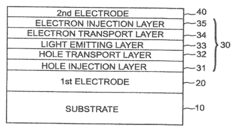
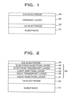
Anode containing metal oxide and organic light emitting device having the same
PatentActiveUS20120326190A1
Innovation
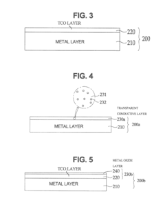
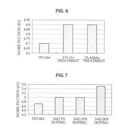
- An anode for organic light emitting devices is developed, comprising a metal layer and a transparent conductive layer with a metal oxide, where the transparent conductive layer includes a mixture of transparent conductive oxides like ITO and metal oxides such as NiO or Co2O3, enhancing the work function and hole injection efficiency, and is formed using sputtering or deposition techniques to achieve optimal thickness and composition for improved reflection and conduction characteristics.
Environmental Impact and Sustainability Considerations
The environmental impact of transparent conductive materials has become increasingly important as electronics production scales globally. Transparent Conductive Oxides (TCOs) and metallic alternatives present distinct environmental profiles throughout their lifecycle. TCOs, particularly Indium Tin Oxide (ITO), face sustainability challenges due to the scarcity of indium, with reserves estimated to last only 20-30 years at current consumption rates. This scarcity drives higher extraction impacts and raises concerns about long-term supply security.
Manufacturing processes for TCOs typically require high-temperature deposition techniques consuming significant energy, with estimates suggesting 30-40% higher energy requirements compared to metallic alternatives. However, TCOs generally exhibit longer operational lifespans in devices, partially offsetting their initial environmental footprint through extended product lifecycles.
Metallic alternatives such as silver nanowire networks and copper meshes offer advantages in resource abundance but present their own environmental challenges. Silver mining and processing generate substantial toxic waste and water pollution, while copper extraction, though less problematic than indium, still contributes to habitat disruption and acid mine drainage in certain regions.
Recent life cycle assessments reveal that metallic solutions typically have lower embodied energy during production but may require more frequent replacement due to oxidation and mechanical degradation, particularly in flexible applications. This creates a complex sustainability equation where initial manufacturing impacts must be balanced against operational longevity.
Recycling capabilities represent another critical sustainability factor. Current electronics recycling systems recover approximately 30-35% of indium from discarded devices, whereas metallic conductors achieve recovery rates of 60-70% through established precious metal recycling channels. This significant difference in end-of-life recoverability influences the overall environmental footprint of these materials.
Water usage presents additional environmental considerations, with TCO production processes typically consuming 1.5-2 times more water than metallic alternatives. However, metallic production often involves more hazardous chemicals requiring specialized treatment and disposal protocols.
Emerging research focuses on developing more sustainable alternatives, including carbon-based conductors and hybrid systems that minimize critical material usage while maintaining performance. These innovations aim to address the environmental limitations of both TCOs and metallic conductors, potentially creating more sustainable pathways for transparent electronics in the future.
Manufacturing Processes and Cost Analysis
The manufacturing processes for transparent conductive oxides (TCOs) and metallic alternatives represent a critical factor in their commercial viability and widespread adoption. TCOs, primarily including indium tin oxide (ITO), aluminum-doped zinc oxide (AZO), and fluorine-doped tin oxide (FTO), are typically produced through physical vapor deposition (PVD) methods such as sputtering, pulsed laser deposition, or chemical vapor deposition (CVD). These processes require high-temperature environments (200-400°C) and sophisticated vacuum equipment, contributing significantly to their overall production costs.
In contrast, metallic alternatives like silver nanowires, copper nanowires, and metal mesh structures can be manufactured using solution-based processes including roll-to-roll printing, spray coating, and spin coating. These methods operate at lower temperatures and often do not require vacuum conditions, potentially reducing energy consumption by 30-50% compared to TCO manufacturing.
Cost analysis reveals that ITO, the most widely used TCO, has a material cost of approximately $600-800 per kilogram, with indium scarcity driving price volatility. The total manufacturing cost for ITO films typically ranges from $15-25 per square meter, including equipment depreciation, energy consumption, and labor. Metal-based alternatives generally offer lower material costs, with silver nanowire solutions priced at $10-15 per square meter, though silver's inherent value keeps costs from decreasing dramatically.
Production scalability presents another significant difference. TCO manufacturing processes face limitations in scaling to very large substrates due to vacuum chamber size constraints and uniformity challenges across large areas. Metal-based alternatives utilizing solution processing methods demonstrate superior scalability potential, with some roll-to-roll processes achieving throughput rates of 10-20 meters per minute compared to 1-3 meters per minute for typical TCO sputtering lines.
Yield rates and defect management also impact overall manufacturing economics. TCO processes typically achieve 85-90% yield rates in mature production lines, while newer metal-based technologies currently demonstrate more variable yields (70-85%), though this gap is narrowing as manufacturing processes mature and optimization continues.
Environmental considerations further differentiate these technologies. TCO production generally consumes more energy and may involve toxic precursors, while metal-based alternatives often utilize less energy-intensive processes but may require more complex recycling systems to recover precious metals from manufacturing waste streams. Recent life cycle assessments indicate that metal mesh technologies can reduce carbon footprint by 15-25% compared to traditional ITO manufacturing when considering the entire production process.
Unlock deeper insights with Patsnap Eureka Quick Research — get a full tech report to explore trends and direct your research. Try now!
Generate Your Research Report Instantly with AI Agent
Supercharge your innovation with Patsnap Eureka AI Agent Platform!