Transparent Conductive Oxides for Electromagnetic Interference Shielding
OCT 27, 20259 MIN READ
Generate Your Research Report Instantly with AI Agent
Patsnap Eureka helps you evaluate technical feasibility & market potential.
TCO EMI Shielding Background and Objectives
Transparent Conductive Oxides (TCOs) have emerged as a critical class of materials at the intersection of optoelectronics and electromagnetic interference (EMI) shielding technologies. The evolution of TCOs began in the early 20th century with the discovery of tin-doped indium oxide (ITO), but their application for EMI shielding has gained significant momentum only in the past two decades, driven by the proliferation of electronic devices and the increasing need for electromagnetic compatibility.
The technological trajectory of TCOs has been shaped by the dual requirements of optical transparency and electrical conductivity—properties that are inherently contradictory in conventional materials. This paradoxical combination makes TCOs uniquely suited for applications where visibility and electromagnetic functionality must coexist, such as in display technologies, smart windows, and now increasingly in EMI shielding solutions.
Recent advancements in nanomaterial science and thin-film deposition techniques have accelerated the development of TCOs with enhanced EMI shielding capabilities. The incorporation of nanostructures, such as nanowires, nanoparticles, and graphene-based composites, has enabled the creation of TCO films with superior conductivity while maintaining high optical transmittance in the visible spectrum.
The primary technical objective of TCO-based EMI shielding research is to achieve a delicate balance between three critical parameters: high optical transparency (typically >80% in the visible range), sufficient electrical conductivity (sheet resistance <100 Ω/sq), and effective EMI shielding efficiency (>20 dB across relevant frequency bands). Additionally, there is a growing emphasis on developing environmentally sustainable alternatives to indium-based TCOs, given the scarcity and high cost of indium.
Industry trends indicate a shift toward flexible, lightweight, and cost-effective TCO solutions that can be integrated into next-generation electronic devices, including foldable displays, wearable technology, and Internet of Things (IoT) sensors. The miniaturization of electronic components and the increasing operating frequencies of wireless communication systems (particularly with the advent of 5G and beyond) have further intensified the need for advanced TCO-based EMI shielding materials.
From a broader perspective, the development of TCOs for EMI shielding aligns with the global push toward digitalization and connectivity, while addressing the growing concerns about electromagnetic pollution and its potential health implications. The convergence of these technological and societal factors underscores the strategic importance of TCO research in enabling the next wave of electronic innovation while ensuring electromagnetic compatibility in increasingly crowded spectral environments.
Market Analysis for Transparent EMI Shielding Solutions
The global market for transparent EMI shielding solutions is experiencing robust growth, driven by the increasing integration of electronic devices across various industries. The market size was valued at approximately $5.6 billion in 2022 and is projected to reach $8.9 billion by 2028, representing a compound annual growth rate (CAGR) of 8.1% during the forecast period.
Consumer electronics remains the dominant application segment, accounting for nearly 40% of the market share. This is primarily attributed to the rising demand for smartphones, tablets, and wearable devices that require effective EMI shielding without compromising display visibility. The automotive sector follows closely, with a market share of around 25%, as modern vehicles incorporate more electronic components and displays requiring transparent EMI protection.
Regionally, Asia-Pacific leads the market with approximately 45% share, owing to the presence of major electronics manufacturing hubs in countries like China, South Korea, Japan, and Taiwan. North America and Europe hold significant shares of 25% and 20% respectively, driven by technological advancements and stringent EMI regulations in these regions.
Transparent conductive oxides (TCOs) are gaining substantial traction within this market, with indium tin oxide (ITO) currently dominating with over 60% market share among transparent conductive materials used for EMI shielding. However, alternative TCOs such as aluminum-doped zinc oxide (AZO) and fluorine-doped tin oxide (FTO) are experiencing faster growth rates due to cost advantages and reduced supply chain risks associated with indium scarcity.
Key market drivers include the proliferation of 5G technology, increasing electromagnetic pollution, stringent regulatory standards, and growing demand for transparent displays in automotive and aerospace applications. The trend toward miniaturization of electronic devices further accelerates the need for effective transparent EMI shielding solutions.
Customer requirements are evolving toward materials that offer higher optical transparency (>90%), lower sheet resistance (<10 ohms/sq), flexibility for curved displays, and environmental sustainability. Price sensitivity varies across application segments, with consumer electronics manufacturers being more cost-conscious compared to aerospace and defense sectors where performance is prioritized over cost.
Market challenges include the high cost of premium transparent conductive materials, technical difficulties in achieving optimal balance between optical transparency and EMI shielding effectiveness, and environmental concerns related to certain manufacturing processes. These factors create significant opportunities for innovation in alternative TCO materials and composite solutions that can address these limitations while meeting performance requirements.
Current TCO Technology Landscape and Challenges
Transparent Conductive Oxides (TCOs) represent a critical class of materials in modern electronics, combining optical transparency with electrical conductivity. The current TCO landscape is dominated by indium tin oxide (ITO), which holds approximately 60% of the global market share due to its excellent balance of transparency (>85% in visible spectrum) and conductivity (sheet resistance <100 Ω/sq). However, ITO faces significant challenges including indium scarcity, rising costs (increased by 25% in the last five years), and brittleness that limits its application in flexible electronics.
Alternative TCOs gaining traction include fluorine-doped tin oxide (FTO), aluminum-doped zinc oxide (AZO), and gallium-doped zinc oxide (GZO). FTO demonstrates superior thermal stability and cost-effectiveness compared to ITO, though with slightly lower optical transparency. AZO and GZO offer comparable optical properties to ITO with improved abundance of raw materials, but face challenges in humidity resistance and long-term stability.
The emerging field of electromagnetic interference (EMI) shielding presents unique requirements for TCOs beyond traditional applications. Effective EMI shielding typically requires conductivity levels of 1-10 S/cm, which many current TCOs struggle to achieve while maintaining >80% optical transparency. This fundamental trade-off between conductivity and transparency represents the central technical challenge in developing TCOs specifically for EMI shielding applications.
Recent innovations include the development of TCO nanocomposites, where conductive nanostructures (such as silver nanowires or carbon nanotubes) are integrated with traditional TCO materials. These hybrid approaches have demonstrated promising EMI shielding effectiveness of 20-30 dB while maintaining optical transparency above 75% in the visible spectrum. However, manufacturing scalability and long-term reliability remain significant hurdles.
Geographically, TCO technology development shows distinct patterns. East Asia (particularly Japan, South Korea, and China) dominates commercial production, accounting for approximately 70% of global TCO manufacturing capacity. North America and Europe lead in research innovation, with significant patent activity focused on novel TCO compositions and deposition techniques optimized for specialized applications including EMI shielding.
The technical limitations currently constraining TCO adoption for EMI shielding include insufficient conductivity at high transparency, limited frequency range effectiveness (typically optimized for either low or high frequencies, but rarely both), and challenges in deposition uniformity over large areas. Additionally, most TCOs exhibit poor mechanical flexibility, with crack formation occurring at strain levels as low as 2-3%, severely limiting their application in next-generation flexible electronics requiring EMI protection.
Contemporary TCO-based EMI Shielding Approaches
01 Transparent conductive oxide films for EMI shielding
Transparent conductive oxide films can be used for electromagnetic interference shielding while maintaining optical transparency. These films typically consist of materials like indium tin oxide (ITO), zinc oxide, or aluminum-doped zinc oxide that provide both electrical conductivity and optical transparency. The films can be deposited on various substrates using techniques such as sputtering or chemical vapor deposition to create effective EMI shields for electronic displays and devices.- Transparent conductive oxide compositions for EMI shielding: Various transparent conductive oxide compositions can be used for electromagnetic interference (EMI) shielding applications. These compositions typically include indium tin oxide (ITO), zinc oxide, or other metal oxides that provide both transparency to visible light and electrical conductivity. The specific composition and doping levels can be optimized to achieve the desired balance between optical transparency and EMI shielding effectiveness.
- Multilayer structures incorporating transparent conductive oxides: Multilayer structures that incorporate transparent conductive oxide layers can provide enhanced EMI shielding performance while maintaining optical transparency. These structures may include alternating layers of different materials, such as conductive oxides combined with polymers or other dielectric materials. The multilayer approach allows for tuning of both the optical and electromagnetic properties of the shielding material.
- Fabrication methods for transparent conductive oxide EMI shields: Various fabrication methods can be employed to create transparent conductive oxide layers for EMI shielding applications. These methods include sputtering, chemical vapor deposition, sol-gel processing, and other thin film deposition techniques. The processing parameters significantly affect the microstructure, conductivity, and transparency of the resulting oxide layers, which in turn determine their EMI shielding effectiveness.
- Integration of transparent conductive oxides in electronic devices: Transparent conductive oxide EMI shields can be integrated into various electronic devices, including displays, touch screens, and photovoltaic cells. The integration methods must address challenges such as adhesion to substrates, durability, and compatibility with other device components. Proper integration ensures that the EMI shielding function does not compromise the device's performance or appearance.
- Grounding and connectivity solutions for transparent conductive oxide shields: Effective grounding and electrical connectivity are essential for transparent conductive oxide EMI shields to function properly. Various techniques can be employed to establish reliable electrical connections to the transparent conductive layers, including conductive adhesives, metal clips, and specialized contact designs. These connections must maintain low resistance while preserving the optical and mechanical properties of the shielding material.
02 Multilayer structures with transparent conductive oxides for enhanced EMI shielding
Multilayer structures incorporating transparent conductive oxide layers can provide enhanced electromagnetic interference shielding. These structures typically combine transparent conductive oxide layers with other materials such as metal meshes, conductive polymers, or dielectric layers. The multilayer approach allows for optimization of both optical transparency and EMI shielding effectiveness across a wide frequency range, making these structures suitable for applications in displays, touch panels, and other electronic devices requiring both visibility and protection from electromagnetic radiation.Expand Specific Solutions03 Patterned transparent conductive oxide structures for EMI shielding
Patterned transparent conductive oxide structures can be designed to provide effective electromagnetic interference shielding while maintaining high optical transparency. These structures typically feature grid patterns, mesh designs, or other geometric configurations that are optimized to block electromagnetic radiation while allowing visible light to pass through. The patterning can be achieved through techniques such as photolithography, laser ablation, or printing methods, enabling customization of the shielding properties for specific applications in displays, windows, or electronic enclosures.Expand Specific Solutions04 Composite materials combining transparent conductive oxides with other materials for EMI shielding
Composite materials that combine transparent conductive oxides with other materials can provide enhanced electromagnetic interference shielding properties. These composites may incorporate conductive polymers, carbon nanomaterials, metal nanoparticles, or other functional additives to improve the overall shielding effectiveness while maintaining optical transparency. The synergistic effects between the transparent conductive oxides and the additional materials can result in broader frequency coverage and higher shielding efficiency, making these composites suitable for applications in portable electronics, aerospace, and medical devices.Expand Specific Solutions05 Manufacturing methods for transparent conductive oxide EMI shielding materials
Various manufacturing methods can be employed to produce transparent conductive oxide materials for electromagnetic interference shielding applications. These methods include physical vapor deposition, chemical vapor deposition, sol-gel processing, and spray coating techniques. Each method offers different advantages in terms of film quality, production cost, and scalability. Advanced processing techniques such as atmospheric plasma treatment or post-deposition annealing can further enhance the electrical conductivity and optical transparency of these materials, improving their effectiveness as EMI shields for electronic devices and displays.Expand Specific Solutions
Leading Manufacturers and Research Institutions
The electromagnetic interference (EMI) shielding market using Transparent Conductive Oxides (TCOs) is currently in a growth phase, with increasing demand driven by the proliferation of electronic devices and wireless technologies. The global market is expanding rapidly, estimated to reach several billion dollars by 2025, with a CAGR of approximately 5-7%. Technologically, TCOs for EMI shielding are advancing from early commercial applications toward broader implementation. Leading companies like Samsung Electronics, AGC Inc., and TDK Corp. are developing advanced TCO solutions with improved transparency and conductivity. Research institutions including Oregon State University and ICFO are pushing boundaries in nanomaterial integration, while specialized materials companies such as Cambrios Technologies and Heraeus are commercializing innovative TCO formulations that balance optical transparency with effective EMI shielding capabilities.
AGC, Inc. (Japan)
Technical Solution: AGC has developed a sophisticated transparent conductive oxide technology platform specifically designed for electromagnetic interference shielding applications. Their approach centers on advanced indium-free TCO formulations, primarily utilizing aluminum-doped zinc oxide (AZO) and fluorine-doped tin oxide (FTO) materials engineered at the nanoscale. AGC's proprietary manufacturing process employs atmospheric pressure chemical vapor deposition (AP-CVD) to create uniform, highly crystalline TCO films with precisely controlled thickness and dopant profiles. These films achieve sheet resistances below 8 ohms/square while maintaining optical transparency exceeding 85% in the visible spectrum. The company has pioneered multilayer TCO structures that incorporate gradient doping profiles and interface engineering to optimize both optical and electrical properties simultaneously. AGC's TCO-based EMI shielding solutions have demonstrated attenuation exceeding 25dB across the 800MHz-5GHz frequency range, making them particularly suitable for telecommunications applications. Their technology has been successfully implemented in architectural glass, automotive displays, and specialty electronics requiring both transparency and EMI protection.
Strengths: World-leading glass manufacturing expertise; established large-area coating capabilities; strong position in architectural and automotive markets; advanced materials characterization capabilities. Weaknesses: Higher production costs compared to traditional metallic EMI shields; limited flexibility for curved or flexible applications; performance degradation at extremely high frequencies.
Samsung Electronics Co., Ltd.
Technical Solution: Samsung has developed advanced transparent conductive oxide (TCO) films specifically engineered for electromagnetic interference (EMI) shielding applications in consumer electronics. Their proprietary technology utilizes indium tin oxide (ITO) and aluminum-doped zinc oxide (AZO) composites with precisely controlled thickness and conductivity profiles. Samsung's approach involves multi-layer TCO structures that achieve both high optical transparency (>85% in the visible spectrum) and effective EMI shielding (>30dB attenuation across 1-10GHz frequency range). The company has integrated these materials into their flagship smartphones and display technologies, creating a seamless EMI shield that doesn't compromise device aesthetics or display quality. Samsung's manufacturing process employs advanced sputtering techniques with precise control over oxygen partial pressure and post-deposition annealing to optimize the microstructure for balanced conductivity and transparency properties.
Strengths: Vertical integration allowing direct implementation in consumer products; extensive manufacturing infrastructure for large-scale production; proven real-world application in commercial devices. Weaknesses: Relatively high production costs; dependence on indium, which faces supply constraints; limited flexibility for non-display applications.
Critical Patents and Technical Innovations in TCO Shielding
Electroconductive laminate, manufacturing process thereof, electromagnetic wave shielding film and protective plate for plasma display
PatentInactiveEP1819210B1
Innovation
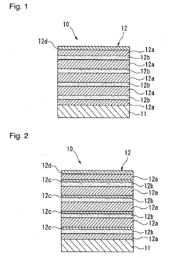
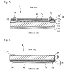
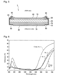
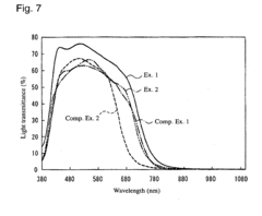
- The electroconductive laminate features a multilayer structure with 2 to 8 metal layers, primarily made of pure silver or silver alloys, and oxide layers containing titanium oxide and zinc oxide, which are alternately laminated on a substrate, along with a protective film to enhance moisture resistance and maintain low resistance.
Plasmonic/transition metal carbo-chalcogenides coating for a flexible, deep and multi-bands electromagnetic interference shielding application
PatentPendingUS20250159852A1
Innovation
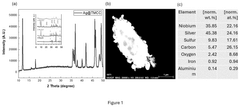
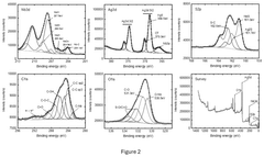
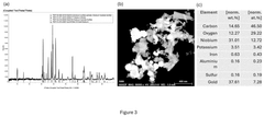
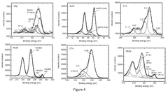
- A composite material comprising an electrically conductive nanoscale film with transition metal carbo-chalcogenides (TMCs) stack layers, decorated with noble metal nanoparticles such as Au, Ag, and Pd, to enhance EMI shielding efficiency.
Material Sustainability and Environmental Impact
The sustainability aspects of Transparent Conductive Oxides (TCOs) for electromagnetic interference (EMI) shielding applications present both challenges and opportunities in the context of environmental impact. Traditional EMI shielding materials often contain heavy metals and environmentally harmful substances, whereas TCOs offer a potentially more sustainable alternative when properly developed and implemented.
The life cycle assessment of TCO materials reveals varying environmental footprints depending on the specific oxide composition. Indium-based TCOs, particularly Indium Tin Oxide (ITO), raise significant sustainability concerns due to indium's scarcity in the Earth's crust and its classification as a critical raw material. Current estimates suggest that indium reserves may face depletion within decades at current consumption rates, driving research toward alternative TCO formulations.
Alternative TCOs based on more abundant elements such as zinc, aluminum, and titanium demonstrate improved sustainability profiles. Zinc-based TCOs, including Aluminum-doped Zinc Oxide (AZO) and Gallium-doped Zinc Oxide (GZO), utilize more widely available resources and typically require lower processing temperatures, resulting in reduced energy consumption during manufacturing.
Manufacturing processes for TCOs also present environmental considerations. Conventional deposition methods like sputtering and chemical vapor deposition often involve high energy consumption and may utilize environmentally harmful precursors. Recent advances in solution-based processing techniques, including sol-gel methods and spray pyrolysis, offer reduced environmental impact through lower processing temperatures and decreased use of toxic solvents.
End-of-life management for TCO-based EMI shielding represents another critical sustainability factor. The integration of TCOs into complex electronic assemblies can complicate recycling efforts. Research into design-for-disassembly approaches and specialized recycling technologies for TCO recovery shows promise for improving circular economy metrics for these materials.
The durability and longevity of TCO-based EMI shielding solutions directly impact their environmental footprint. Materials that maintain performance over extended periods reduce replacement frequency and associated resource consumption. Recent developments in protective coatings and composite structures have enhanced TCO durability in harsh environments, extending useful lifespans and improving overall sustainability metrics.
Regulatory frameworks increasingly influence TCO material selection and processing. The European Union's Restriction of Hazardous Substances (RoHS) directive and Registration, Evaluation, Authorization and Restriction of Chemicals (REACH) regulations have accelerated the transition away from certain toxic elements in TCO formulations, driving innovation toward greener alternatives that maintain effective EMI shielding performance while minimizing environmental harm.
Integration Strategies for Electronics Applications
The integration of Transparent Conductive Oxides (TCOs) into electronic devices for electromagnetic interference (EMI) shielding requires sophisticated strategies that balance optical transparency, electrical conductivity, and manufacturing feasibility. Current integration approaches primarily focus on thin-film deposition techniques, with physical vapor deposition (PVD) and chemical vapor deposition (CVD) being the most prevalent methods for applying TCO layers to electronic components.
Sputtering, a PVD technique, offers precise control over film thickness and composition, making it ideal for depositing indium tin oxide (ITO) and aluminum-doped zinc oxide (AZO) on sensitive electronic substrates. This method enables the creation of uniform TCO layers with thicknesses ranging from 50 to 300 nm, providing effective EMI shielding while maintaining optical transparency above 80% in the visible spectrum.
Solution-based deposition methods, including sol-gel processing and spray pyrolysis, represent cost-effective alternatives for large-area applications. These techniques are particularly valuable for flexible electronics, where traditional vacuum-based methods may cause thermal stress or damage. Recent advancements in solution processing have yielded TCO films with sheet resistances below 100 Ω/sq while maintaining transparency above 85%.
For three-dimensional electronic components, conformal coating techniques have been developed to ensure uniform TCO coverage. Atomic layer deposition (ALD) stands out in this regard, offering angstrom-level precision in layer thickness and excellent step coverage, though at the cost of slower deposition rates compared to other methods.
Post-deposition treatments significantly enhance TCO performance in EMI shielding applications. Thermal annealing at temperatures between 300-500°C improves crystallinity and reduces defects, thereby enhancing electrical conductivity. For temperature-sensitive substrates, photonic curing and laser annealing provide viable alternatives, enabling rapid processing without substrate damage.
Multilayer architectures represent an advanced integration strategy, where TCO layers are combined with other functional materials to create composite shielding systems. TCO/metal/TCO sandwiches have demonstrated superior EMI shielding effectiveness (>30 dB) while maintaining optical transparency above 70%. These structures leverage the high conductivity of ultrathin metal layers while preserving transparency through the surrounding TCO layers.
Interface engineering between TCOs and device substrates remains crucial for long-term reliability. Adhesion promoters and buffer layers help mitigate thermal expansion mismatches and prevent delamination during thermal cycling. Additionally, encapsulation technologies protect TCO layers from environmental degradation, extending device lifetime in harsh operating conditions.
Unlock deeper insights with Patsnap Eureka Quick Research — get a full tech report to explore trends and direct your research. Try now!
Generate Your Research Report Instantly with AI Agent
Supercharge your innovation with Patsnap Eureka AI Agent Platform!
