Research on Transparent Conductive Oxides and Coating Technologies
OCT 27, 20259 MIN READ
Generate Your Research Report Instantly with AI Agent
Patsnap Eureka helps you evaluate technical feasibility & market potential.
TCO Background and Development Objectives
Transparent Conductive Oxides (TCOs) represent a critical class of materials that combine electrical conductivity with optical transparency, properties that are inherently contradictory in conventional materials. The development of TCOs began in the early 20th century with the discovery of cadmium oxide's conductive properties, but significant advancements emerged in the 1970s with the introduction of indium tin oxide (ITO). This material revolutionized display technologies and remains the industry standard despite ongoing challenges.
The evolution of TCO materials has been driven by the exponential growth of optoelectronic devices, particularly touchscreens, flat panel displays, photovoltaic cells, and smart windows. The global TCO market has expanded at a compound annual growth rate exceeding 10% over the past decade, reflecting the increasing integration of these materials in consumer electronics and renewable energy applications.
Current technological development focuses on addressing several critical limitations of existing TCO materials. The scarcity and high cost of indium have prompted intensive research into alternative materials such as fluorine-doped tin oxide (FTO), aluminum-doped zinc oxide (AZO), and more recently, graphene-based composites. Additionally, there is growing emphasis on developing TCOs with enhanced flexibility to support the emerging flexible electronics market.
The environmental impact of TCO production processes has also become a significant consideration, with research efforts directed toward developing eco-friendly deposition methods and reducing the use of rare or toxic elements. This aligns with global sustainability initiatives and regulatory frameworks governing electronic waste management.
The primary technical objectives for TCO research include achieving higher transparency in the visible spectrum (>90%) while maintaining electrical conductivity below 10^-3 Ω·cm, enhancing mechanical flexibility without compromising performance, and developing cost-effective, scalable manufacturing processes. These objectives are particularly challenging as they often involve trade-offs between optical, electrical, and mechanical properties.
Another crucial development goal is improving the stability of TCO materials under various environmental conditions, including humidity, temperature fluctuations, and UV exposure. This is essential for extending the operational lifespan of devices incorporating these materials, particularly in outdoor applications such as solar cells and smart architectural elements.
The convergence of nanotechnology with TCO research has opened new avenues for material design, enabling precise control over composition, structure, and interface properties at the nanoscale. This approach promises to overcome current limitations and potentially discover entirely new classes of transparent conductive materials with superior performance characteristics.
Market Analysis for Transparent Conductive Materials
The transparent conductive materials market has witnessed substantial growth over the past decade, primarily driven by the expanding electronics industry and increasing demand for touchscreen devices. The global market for transparent conductive materials was valued at approximately 4.8 billion USD in 2022 and is projected to reach 8.3 billion USD by 2028, growing at a CAGR of 9.5% during the forecast period.
Indium Tin Oxide (ITO) continues to dominate the market with over 70% market share due to its excellent combination of optical transparency and electrical conductivity. However, the limited availability and rising cost of indium have prompted manufacturers to seek alternative materials, creating significant market opportunities for emerging technologies such as silver nanowires, carbon nanotubes, graphene, and metal mesh structures.
The consumer electronics segment represents the largest application area, accounting for nearly 55% of the market share. Smartphones, tablets, and laptops collectively drive substantial demand for transparent conductive materials. The automotive industry is emerging as a rapidly growing segment, with increasing integration of touch panels and displays in vehicle interiors contributing to market expansion.
Geographically, Asia-Pacific leads the market with approximately 65% share, primarily due to the concentration of electronics manufacturing facilities in countries like China, South Korea, Japan, and Taiwan. North America and Europe follow with 18% and 12% market shares respectively, with growing adoption in specialized applications such as photovoltaics and smart architecture.
The photovoltaic sector represents a particularly promising growth area, with transparent conductive oxides being essential components in thin-film solar cells. This segment is expected to grow at a CAGR of 12% through 2028, outpacing the overall market growth rate.
Key market trends include increasing R&D investments in flexible and stretchable transparent conductors to support the growing demand for foldable displays and wearable electronics. Additionally, sustainability concerns are driving research into environmentally friendly alternatives to traditional TCO materials, with reduced energy consumption during manufacturing and improved recyclability.
Price sensitivity remains a critical factor in market dynamics, with manufacturers continuously seeking cost-effective solutions without compromising performance. This has accelerated innovation in coating technologies that can reduce material usage while maintaining or improving functional properties.
Current TCO Technology Landscape and Challenges
Transparent Conductive Oxides (TCOs) currently dominate the transparent electrode market, with Indium Tin Oxide (ITO) maintaining its position as the industry standard despite emerging alternatives. ITO offers an exceptional combination of high optical transparency (>90%) and low electrical resistivity (<10^-4 Ω·cm), making it ideal for applications in displays, photovoltaics, and smart windows. However, the global landscape faces significant challenges due to indium's scarcity and geopolitical supply constraints, with over 70% of global reserves concentrated in China, creating price volatility and supply chain vulnerabilities.
The manufacturing ecosystem for TCOs has evolved significantly, with major production facilities established across East Asia, particularly in Japan, South Korea, and Taiwan. Sputtering remains the predominant deposition technique for commercial TCO production, accounting for approximately 65% of industrial applications, while chemical vapor deposition (CVD) and sol-gel methods represent growing alternatives for specific applications requiring conformal coatings or lower capital investment.
Technical challenges persist in achieving the ideal balance between transparency and conductivity, as these properties are fundamentally coupled through carrier concentration effects. Current state-of-the-art TCOs struggle to maintain performance when subjected to mechanical stress, with typical ITO films experiencing conductivity degradation of 50-80% at bending radii below 10mm, severely limiting applications in flexible electronics.
Environmental and sustainability concerns represent another significant challenge, with conventional TCO manufacturing processes requiring high temperatures (typically 300-400°C) and vacuum conditions, resulting in substantial energy consumption and carbon footprint. Additionally, the etching processes used in patterning often employ environmentally hazardous chemicals such as hydrochloric acid and aqua regia.
Alternative TCO materials such as aluminum-doped zinc oxide (AZO), fluorine-doped tin oxide (FTO), and indium-free compounds have emerged as potential substitutes, but they currently exhibit 15-30% lower performance in key metrics compared to ITO. These alternatives face adoption barriers including process integration challenges, long-term stability issues, and insufficient economies of scale in production.
The geographical distribution of TCO research and development shows concentration in East Asia (40%), North America (30%), and Europe (25%), with emerging contributions from research institutions in India and Brazil. This distribution largely mirrors manufacturing capabilities, creating potential innovation bottlenecks in regions with limited production infrastructure.
Contemporary TCO Coating Methodologies
01 Indium Tin Oxide (ITO) based transparent conductive films
Indium Tin Oxide (ITO) is widely used as a transparent conductive oxide material for various applications including displays, touch panels, and solar cells. These films offer excellent optical transparency combined with good electrical conductivity. Various deposition methods such as sputtering and chemical vapor deposition are employed to create high-quality ITO films with controlled thickness and properties. The manufacturing processes often focus on optimizing the balance between transparency and conductivity while maintaining durability.- Indium Tin Oxide (ITO) based transparent conductive films: Indium Tin Oxide (ITO) is widely used as a transparent conductive oxide material for various applications including displays, touch panels, and solar cells. These films offer high transparency in the visible light range while maintaining good electrical conductivity. Various deposition methods such as sputtering and chemical vapor deposition are employed to create uniform ITO films with controlled thickness and properties. The electrical and optical properties can be tuned by adjusting the indium to tin ratio and processing conditions.
- Alternative transparent conductive oxide materials: Due to the scarcity and high cost of indium, alternative transparent conductive oxide materials have been developed. These include zinc oxide-based materials (such as AZO - aluminum-doped zinc oxide), fluorine-doped tin oxide (FTO), and other metal oxides that can provide similar optical transparency and electrical conductivity. These alternative materials often offer advantages such as lower cost, improved stability, or better performance in specific applications like flexible electronics or photovoltaics.
- Nanostructured transparent conductive coatings: Nanostructured transparent conductive coatings incorporate nanomaterials such as carbon nanotubes, graphene, metal nanowires, or nanoparticles to achieve transparency and conductivity. These materials can be deposited as networks or composite structures that allow light to pass through while providing electrical pathways. Nanostructured coatings often offer advantages such as flexibility, stretchability, and compatibility with roll-to-roll manufacturing processes, making them suitable for next-generation flexible electronics and displays.
- Deposition and coating technologies for transparent conductive films: Various deposition and coating technologies are employed to create transparent conductive oxide films with controlled properties. These include physical vapor deposition methods (sputtering, evaporation), chemical vapor deposition, sol-gel processes, and solution-based coating techniques. Each method offers different advantages in terms of film quality, throughput, cost, and compatibility with various substrates. Post-deposition treatments such as annealing or plasma treatment are often used to optimize the electrical and optical properties of the films.
- Applications and device integration of transparent conductive oxides: Transparent conductive oxides are integrated into various electronic and optoelectronic devices including touch screens, displays, solar cells, smart windows, and LEDs. The integration process involves considerations of substrate compatibility, interface engineering, patterning techniques, and device architecture. Specialized coating designs such as multilayer structures or gradient compositions are developed to meet specific application requirements like high transparency in certain wavelength ranges, low sheet resistance, or environmental stability.
02 Alternative transparent conductive oxide materials
Due to the limited supply and high cost of indium, alternative transparent conductive oxide materials have been developed. These include zinc oxide-based compounds (such as AZO - aluminum-doped zinc oxide), fluorine-doped tin oxide (FTO), and other metal oxide combinations. These alternative materials aim to provide comparable optical and electrical properties to ITO while reducing dependency on rare elements. Research focuses on improving their stability, conductivity, and manufacturing scalability for various electronic and optoelectronic applications.Expand Specific Solutions03 Deposition and coating techniques for transparent conductive oxides
Various deposition techniques are employed for creating transparent conductive oxide coatings, including magnetron sputtering, chemical vapor deposition, sol-gel processes, and spray pyrolysis. Each method offers different advantages in terms of film quality, production cost, and scalability. Advanced techniques focus on achieving uniform coating thickness, minimizing defects, and enabling deposition on flexible or temperature-sensitive substrates. Process parameters such as temperature, pressure, and gas composition are carefully controlled to optimize film properties.Expand Specific Solutions04 Nanostructured transparent conductive materials
Nanostructured transparent conductive materials incorporate nanowires, nanoparticles, or other nanostructures to enhance performance characteristics. These materials can achieve high transparency and conductivity through unique structural arrangements that allow light transmission while providing conductive pathways. Nanomaterials such as silver nanowires, carbon nanotubes, and graphene have been incorporated into transparent conductive films. These approaches often aim to create flexible, stretchable, or otherwise mechanically robust transparent conductors for next-generation electronic devices.Expand Specific Solutions05 Applications and device integration of transparent conductive oxides
Transparent conductive oxides are integrated into various devices including displays, touch panels, solar cells, smart windows, and optoelectronic components. The integration process requires consideration of interface properties, adhesion, patterning techniques, and compatibility with other device layers. Specialized coating designs address application-specific requirements such as flexibility for wearable electronics, durability for outdoor applications, or precise optical properties for display technologies. Advanced manufacturing techniques enable high-throughput production while maintaining quality and performance specifications.Expand Specific Solutions
Leading Companies and Research Institutions in TCO Field
The transparent conductive oxides (TCO) market is currently in a growth phase, with increasing demand driven by applications in displays, photovoltaics, and smart windows. The global market size is estimated to reach $8-10 billion by 2025, growing at a CAGR of approximately 6-8%. Technologically, the field is maturing with established players like AGC, Sumitomo Metal Mining, and Samsung Electronics leading commercial applications, while research institutions such as ITRI, Fudan University, and Oregon State University drive innovation in next-generation materials. Companies like Applied Materials and VON ARDENNE are advancing coating technologies, while specialty chemical firms including Henkel and BASF are developing novel formulations. The competitive landscape shows a balance between large corporations with manufacturing scale and specialized firms focusing on high-performance niche applications, with increasing collaboration between industry and academia to overcome technical challenges in transparency, conductivity, and cost.
Sumitomo Metal Mining Co. Ltd.
Technical Solution: Sumitomo Metal Mining has established itself as a leader in TCO materials development, particularly in ITO target manufacturing for sputtering applications. Their proprietary sintering process creates high-density ITO targets (>99.5% theoretical density) that enable uniform film deposition with minimal particle generation. Sumitomo has developed specialized ITO compositions with dopant modifications that achieve sheet resistance below 8 ohms/sq while maintaining >90% visible light transmission. Their recent innovations include indium-saving TCO materials that incorporate alternative dopants to reduce indium content by up to 30% without compromising electrical performance. Sumitomo's TCO product line extends beyond ITO to include AZO and gallium-doped zinc oxide (GZO) materials optimized for specific applications. Their advanced manufacturing processes ensure exceptional target purity (>99.999%), critical for achieving consistent TCO film properties in high-volume production. Sumitomo has also developed nanoparticle-based TCO inks for printed electronics applications, expanding TCO usage beyond traditional vacuum deposition methods.
Strengths: World-class materials expertise and manufacturing capabilities for TCO target materials; strong vertical integration from raw material refining to finished TCO products. Weaknesses: Primary focus on materials supply rather than complete coating solutions; limited direct engagement in end-application development compared to device manufacturers.
AGC, Inc. (Japan)
Technical Solution: AGC has developed advanced transparent conductive oxide (TCO) technologies focusing on indium tin oxide (ITO) and fluorine-doped tin oxide (FTO) coatings. Their proprietary ATTOCH™ technology enables ultra-thin TCO films with exceptional transparency (>90%) while maintaining conductivity below 10 ohms/sq. AGC employs both magnetron sputtering and chemical vapor deposition methods, allowing versatile application across different substrate types and sizes. Their recent innovation includes the development of damage-resistant TCO films that maintain performance even under mechanical stress, addressing a key limitation in flexible electronics applications. AGC has also pioneered low-temperature deposition processes that enable TCO application on temperature-sensitive substrates like polymers, expanding potential applications in flexible displays and photovoltaics. Their integrated manufacturing approach combines glass production with coating technologies, providing end-to-end solutions for various industries.
Strengths: Vertical integration from glass manufacturing to coating provides complete supply chain control; proprietary deposition technologies enable high-performance TCO films on various substrates. Weaknesses: Heavy reliance on indium, a scarce and expensive material; coating technologies primarily optimized for flat glass applications rather than curved or flexible surfaces.
Key Patents and Innovations in TCO Technology
Method for producing transparent conductive film, transparent conductive film, transparent conductive substrate and device comprising the same
PatentInactiveUS9040119B2
Innovation
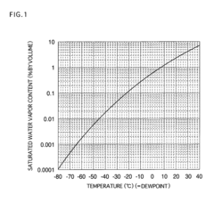
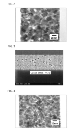
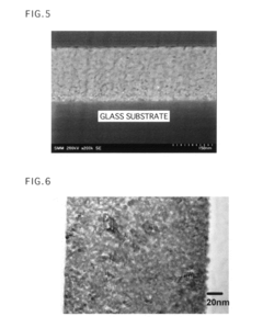
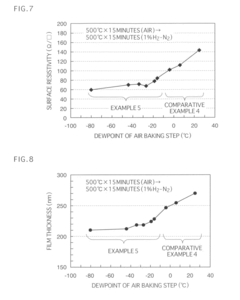
- A method involving coating a heat-resistant substrate with a coating liquid containing organic metal compounds like acetylacetone indium or tin, followed by drying and baking under an oxygen-containing atmosphere with low dewpoint, which inhibits crystal growth and promotes the formation of a densely filled conductive oxide microparticle layer, enhancing both conductivity and film strength.
Transparent conductive film and production method therefor
PatentInactiveUS20150357077A1
Innovation
- A transparent conductive film with a crystalline indium-based complex oxide coating, specifically an indium-tin complex oxide, is formed using high magnetic field RF superimposed DC sputtering deposition with a tetravalent metal element oxide content of 7-15% and a thickness of 10-40 nm, along with a pre-sputtering step and annealing process to achieve low specific and surface resistances.
Environmental Impact and Sustainability of TCO Materials
The environmental impact of Transparent Conductive Oxide (TCO) materials has become increasingly significant as their applications expand across various industries. Traditional TCO manufacturing processes often involve energy-intensive methods and potentially hazardous materials, raising concerns about their overall environmental footprint. The production of indium tin oxide (ITO), the most widely used TCO, requires scarce indium resources, with estimates suggesting that economically viable indium reserves may face depletion within decades if consumption continues at current rates.
Manufacturing processes for TCOs typically involve high-temperature deposition techniques such as sputtering, chemical vapor deposition, or sol-gel methods, all of which consume substantial energy. The carbon footprint associated with these energy-intensive processes contributes significantly to the environmental impact of TCO-based devices. Additionally, certain TCO production methods utilize toxic precursors or generate harmful byproducts, posing risks to both environmental and human health.
Recent sustainability initiatives have focused on developing alternative TCO materials with reduced environmental impact. Zinc oxide-based compounds, fluorine-doped tin oxide (FTO), and carbon-based alternatives like graphene represent promising directions for more sustainable TCO materials. These alternatives often require less energy to produce and utilize more abundant elements, addressing both resource scarcity and energy consumption concerns.
Recycling and recovery of TCO materials present both challenges and opportunities. The thin-film nature of TCO coatings makes them difficult to separate from substrates, complicating end-of-life recovery. However, innovative recycling technologies are emerging, including selective chemical etching and advanced physical separation techniques that can recover valuable elements from discarded electronic devices containing TCO layers.
Life cycle assessment (LCA) studies comparing different TCO materials reveal varying environmental impacts across their production, use, and disposal phases. While ITO typically shows higher environmental impact during production due to indium scarcity and energy-intensive processing, some alternatives may present trade-offs in terms of durability or performance that affect their lifetime environmental footprint.
Regulatory frameworks worldwide are increasingly addressing the sustainability aspects of electronic materials, including TCOs. The European Union's Restriction of Hazardous Substances (RoHS) directive and similar regulations in other regions have pushed manufacturers toward developing more environmentally benign TCO materials and production processes. These regulatory pressures, combined with corporate sustainability initiatives, are accelerating the transition toward greener TCO technologies.
Integration Challenges in Device Manufacturing
The integration of Transparent Conductive Oxides (TCOs) into device manufacturing presents significant challenges that require careful consideration and innovative solutions. One of the primary obstacles is achieving uniform deposition of TCO materials across large substrate areas, particularly for applications in displays and photovoltaics where consistency is crucial for device performance. Variations in thickness and composition can lead to non-uniform electrical and optical properties, compromising overall device efficiency.
Temperature sensitivity poses another critical challenge, as many TCO deposition processes require high temperatures that may damage underlying device components or substrates. This is particularly problematic for flexible electronics and temperature-sensitive organic materials, necessitating the development of low-temperature deposition techniques without sacrificing film quality.
Interface engineering between TCOs and adjacent device layers represents a complex integration challenge. Poor adhesion, chemical incompatibility, or unfavorable band alignment can result in increased contact resistance, reduced charge transfer efficiency, and accelerated device degradation. Specialized interface layers or surface treatments are often required to optimize these critical junctions.
Pattern definition and etching processes for TCOs must be precisely controlled to achieve the desired feature resolution while maintaining material properties. Conventional photolithography and etching techniques may damage TCO films or create undesirable edge effects that impact device performance. Alternative patterning methods such as lift-off processes or laser ablation are being explored to address these limitations.
Mechanical stability presents ongoing concerns, especially for flexible and wearable electronics. TCO films must maintain conductivity under bending, stretching, and repeated mechanical stress without developing microcracks or delamination. This necessitates careful optimization of film thickness, composition, and deposition parameters to enhance durability while preserving functionality.
Environmental stability and encapsulation requirements further complicate integration efforts. Many TCO materials, particularly those containing indium or zinc, are susceptible to degradation when exposed to moisture, oxygen, or elevated temperatures. Effective encapsulation strategies must be developed to protect these materials without adding excessive cost or complexity to the manufacturing process.
Cost-effective scaling of TCO integration remains a significant hurdle for mass production. The industry continues to seek economically viable approaches that maintain material quality and performance while reducing dependence on scarce elements like indium. This includes exploring alternative materials, improving deposition efficiency, and developing recycling methods for valuable TCO components.
Unlock deeper insights with Patsnap Eureka Quick Research — get a full tech report to explore trends and direct your research. Try now!
Generate Your Research Report Instantly with AI Agent
Supercharge your innovation with Patsnap Eureka AI Agent Platform!