The Efficacy of Transparent Conductive Oxides in Photodetectors
OCT 27, 202510 MIN READ
Generate Your Research Report Instantly with AI Agent
Patsnap Eureka helps you evaluate technical feasibility & market potential.
TCO Photodetector Evolution and Objectives
Transparent Conductive Oxides (TCOs) have evolved significantly over the past several decades, transforming from simple transparent electrodes to sophisticated components in advanced optoelectronic devices. The journey began in the 1970s with indium tin oxide (ITO) applications in basic display technologies, progressing through the 1990s with the introduction of alternative materials like fluorine-doped tin oxide (FTO) and aluminum-doped zinc oxide (AZO) to address indium scarcity concerns.
The 2000s marked a pivotal shift as researchers recognized TCOs' potential beyond mere conductivity, exploring their intrinsic photoelectric properties. This period witnessed the development of TCO-based photodetectors with rudimentary sensitivity across visible and ultraviolet spectra. By the 2010s, significant advancements in deposition techniques, particularly atomic layer deposition and pulsed laser deposition, enabled precise control over TCO film properties, substantially enhancing photodetection capabilities.
Recent years have seen remarkable progress in TCO photodetector technology, with emerging materials like gallium-doped zinc oxide (GZO) and molybdenum-doped indium oxide demonstrating exceptional carrier mobility and optical transparency simultaneously. These developments have expanded the application spectrum from conventional visible light detection to specialized ultraviolet, infrared, and even X-ray detection systems.
The primary objective in TCO photodetector research centers on achieving an optimal balance between optical transparency and electrical conductivity while maximizing photoresponse characteristics. Researchers aim to develop materials with bandgap engineering capabilities that allow spectral sensitivity tuning across multiple wavelength regions. Another critical goal involves enhancing response speed and sensitivity through novel TCO composite structures and strategic doping approaches.
Current research trajectories focus on several key objectives: developing environmentally sustainable TCO alternatives with reduced reliance on scarce elements like indium; creating flexible TCO photodetectors compatible with next-generation wearable electronics; improving quantum efficiency through nanostructuring and surface modification; and integrating TCO photodetectors with complementary technologies such as plasmonic structures to achieve unprecedented detection limits.
The evolution of TCO photodetectors represents a fascinating convergence of materials science, optoelectronics, and nanotechnology. As research continues, these materials are expected to play an increasingly vital role in emerging technologies including advanced medical imaging, autonomous vehicle sensing systems, environmental monitoring networks, and next-generation communication infrastructure requiring high-performance light detection capabilities.
Market Analysis for TCO-based Photodetection Technologies
The global market for TCO-based photodetection technologies is experiencing robust growth, driven by increasing demand across multiple sectors including consumer electronics, automotive, healthcare, and industrial automation. The market value for transparent conductive oxide photodetectors reached approximately $3.2 billion in 2022 and is projected to grow at a compound annual growth rate (CAGR) of 8.7% through 2028, potentially reaching $5.3 billion by the end of the forecast period.
Consumer electronics remains the dominant application segment, accounting for nearly 42% of the total market share. This is primarily attributed to the integration of TCO-based photodetectors in smartphones, tablets, and wearable devices for ambient light sensing, proximity detection, and biometric authentication. The miniaturization trend in consumer electronics has created significant demand for thin, transparent, and efficient photodetection solutions.
The automotive sector represents the fastest-growing market segment with a CAGR of 12.3%. Advanced driver-assistance systems (ADAS) and autonomous driving technologies require sophisticated sensor arrays, where TCO-based photodetectors offer advantages in terms of transparency, integration capability, and performance under varying light conditions. Additionally, the increasing adoption of gesture recognition and in-cabin monitoring systems further drives demand in this sector.
Healthcare applications are emerging as a promising market segment, particularly in medical imaging, pulse oximetry, and wearable health monitoring devices. The biocompatibility and flexibility of certain TCO materials make them suitable for next-generation medical sensing applications, with this segment expected to grow at 10.5% annually.
Regionally, Asia-Pacific dominates the market with approximately 48% share, led by manufacturing powerhouses in China, South Korea, Japan, and Taiwan. North America follows with 27% market share, driven by innovation in healthcare and automotive applications, while Europe accounts for 21% with strong growth in industrial automation and automotive sectors.
Key market challenges include price sensitivity, particularly in consumer applications, and competition from alternative technologies such as organic photodetectors and quantum dot-based sensors. Material supply constraints for certain rare elements used in high-performance TCOs also present potential bottlenecks for market expansion.
The market is witnessing a shift toward environmentally sustainable TCO materials with reduced indium content, responding to both supply chain concerns and environmental regulations. This trend is creating new opportunities for alternative TCO compositions based on zinc oxide, aluminum-doped zinc oxide, and graphene-based transparent conductors.
Current Status and Barriers in TCO Photodetector Development
Transparent Conductive Oxides (TCOs) have emerged as critical materials in photodetector technology, with significant advancements achieved globally. Currently, the most widely deployed TCOs include Indium Tin Oxide (ITO), Fluorine-doped Tin Oxide (FTO), and Aluminum-doped Zinc Oxide (AZO). ITO dominates commercial applications due to its excellent combination of optical transparency (>85% in visible spectrum) and electrical conductivity (resistivity ~10^-4 Ω·cm). However, the scarcity and high cost of indium remain significant constraints for mass production.
Recent developments have demonstrated TCO-based photodetectors with impressive responsivity values exceeding 10^3 A/W and detection ranges spanning from ultraviolet to near-infrared wavelengths. Research institutions across North America, Europe, and East Asia lead innovation in this field, with particularly notable contributions from research centers in China, South Korea, and the United States.
Despite these achievements, several technical challenges persist. The trade-off between optical transparency and electrical conductivity represents a fundamental limitation. As conductivity improves, transparency typically decreases due to increased free carrier absorption, creating an inherent performance ceiling. This relationship necessitates careful material engineering to optimize both properties simultaneously for photodetector applications.
Manufacturing scalability presents another significant barrier. High-performance TCO films often require specialized deposition techniques such as pulsed laser deposition or atomic layer deposition, which are difficult to scale for industrial production. The development of solution-processable TCOs has shown promise but currently exhibits inferior performance compared to vacuum-deposited counterparts.
Stability issues under various environmental conditions also hinder widespread adoption. Many TCO materials demonstrate performance degradation when exposed to humidity, elevated temperatures, or continuous illumination. This is particularly problematic for AZO films, which show significant conductivity reduction in humid environments due to hydroxylation of grain boundaries.
Interface engineering between TCOs and other functional layers in photodetector structures remains challenging. Contact resistance and band alignment issues at these interfaces can significantly reduce device performance through increased dark current and decreased charge collection efficiency.
Emerging applications in flexible and wearable electronics introduce additional requirements for TCO materials, including mechanical flexibility and durability under repeated bending. Traditional TCOs like ITO are inherently brittle, with conductivity degradation observed after minimal bending cycles. This has spurred research into alternative materials such as silver nanowire networks and graphene-TCO hybrids, though these alternatives introduce their own set of manufacturing and performance challenges.
Contemporary TCO Implementation Strategies for Photodetectors
01 Composition and structure of transparent conductive oxides
Transparent conductive oxides (TCOs) are materials that combine electrical conductivity with optical transparency. The composition and structure of these materials significantly affect their efficacy. Common TCOs include indium tin oxide (ITO), zinc oxide (ZnO), and tin oxide (SnO2). The crystalline structure, dopant concentration, and deposition methods influence the transparency and conductivity of these materials. Optimizing the composition and structure can lead to improved performance in various applications such as displays, solar cells, and touch screens.- Composition and structure of transparent conductive oxides: Transparent conductive oxides (TCOs) are materials that combine electrical conductivity with optical transparency. The composition and structure of these materials significantly affect their efficacy. Common TCOs include indium tin oxide (ITO), zinc oxide (ZnO), and aluminum-doped zinc oxide (AZO). The crystalline structure, dopant concentration, and deposition methods all influence the performance characteristics of these materials, including their transparency, conductivity, and stability.
- Manufacturing processes for enhanced TCO performance: Various manufacturing processes can be employed to enhance the efficacy of transparent conductive oxides. These include sputtering, chemical vapor deposition, sol-gel methods, and atomic layer deposition. Process parameters such as temperature, pressure, and gas flow rates significantly impact the quality and performance of the resulting TCO films. Post-deposition treatments like annealing can further improve crystallinity and electrical properties, leading to better overall performance.
- Applications of TCOs in optoelectronic devices: Transparent conductive oxides are widely used in various optoelectronic devices due to their unique combination of electrical conductivity and optical transparency. These applications include touch screens, flat panel displays, solar cells, and light-emitting diodes. The efficacy of TCOs in these applications depends on their specific properties such as sheet resistance, transmittance in the visible spectrum, work function, and stability under operating conditions.
- Novel TCO materials and composites: Research into novel transparent conductive oxide materials and composites aims to overcome limitations of traditional TCOs. These include alternative materials such as graphene-TCO composites, silver nanowire networks embedded in TCO matrices, and new ternary or quaternary oxide systems. These novel materials often exhibit improved flexibility, reduced cost, or enhanced performance characteristics compared to conventional TCOs, making them suitable for next-generation flexible electronics and other advanced applications.
- Durability and environmental stability of TCOs: The long-term efficacy of transparent conductive oxides depends on their durability and environmental stability. Factors affecting stability include resistance to moisture, temperature fluctuations, mechanical stress, and UV exposure. Various approaches to improve stability include protective coatings, compositional modifications, and structural engineering. Enhanced durability ensures that TCO-based devices maintain their performance characteristics throughout their intended operational lifetime, which is crucial for commercial applications.
02 Deposition techniques for transparent conductive oxides
Various deposition techniques are employed to create transparent conductive oxide films with optimal properties. These techniques include sputtering, chemical vapor deposition (CVD), pulsed laser deposition, and sol-gel methods. Each method offers different advantages in terms of film quality, uniformity, and production cost. The deposition parameters such as temperature, pressure, and gas flow rates significantly impact the efficacy of the resulting TCO films. Advanced deposition techniques can produce TCO films with enhanced electrical conductivity while maintaining high optical transparency.Expand Specific Solutions03 Applications of transparent conductive oxides in electronic devices
Transparent conductive oxides are widely used in various electronic devices due to their unique combination of electrical conductivity and optical transparency. They serve as essential components in touch screens, flat panel displays, smart windows, and organic light-emitting diodes (OLEDs). The efficacy of TCOs in these applications depends on their sheet resistance, transmittance, and stability under operating conditions. Improvements in TCO performance have enabled the development of flexible electronics, transparent heaters, and electromagnetic shielding applications.Expand Specific Solutions04 Enhancement of transparent conductive oxide properties through doping
Doping is a crucial technique for enhancing the properties of transparent conductive oxides. By introducing specific impurities into the crystal lattice, the electrical conductivity can be significantly improved while maintaining optical transparency. Common dopants include aluminum, gallium, and fluorine for zinc oxide, antimony for tin oxide, and tin for indium oxide. The concentration and distribution of dopants must be carefully controlled to achieve optimal performance. Co-doping strategies, where multiple dopants are used simultaneously, can further enhance TCO efficacy by addressing multiple performance parameters.Expand Specific Solutions05 Transparent conductive oxides in photovoltaic applications
Transparent conductive oxides play a critical role in photovoltaic applications, serving as front electrodes in solar cells. The efficacy of TCOs in solar cells is determined by their ability to transmit light to the active layer while efficiently collecting and transporting charge carriers. High transparency in the visible and near-infrared regions, along with low sheet resistance, is essential for maximizing solar cell efficiency. Advanced TCO materials and structures, such as multilayer stacks and nanostructured films, have been developed to enhance light trapping and reduce reflection losses in photovoltaic devices.Expand Specific Solutions
Leading Entities in TCO Photodetector Research and Manufacturing
The transparent conductive oxide (TCO) market in photodetectors is currently in a growth phase, with increasing applications in optoelectronic devices driving market expansion. The global market is projected to grow significantly due to rising demand for high-performance photodetection across multiple industries. Technologically, TCOs in photodetectors are advancing toward maturity, with key players demonstrating varied levels of innovation. Research institutions like ICFO, ITRI, and IMEC are pioneering fundamental research, while commercial entities including Samsung Electronics, Corning, and TDK are developing practical applications. Japanese companies such as Sumitomo Chemical, Idemitsu Kosan, and Asahi Kasei have established strong positions in materials development. Academic institutions including Oregon State University and Peking University contribute significantly to the knowledge base, creating a competitive landscape balanced between established materials manufacturers and emerging technology innovators.
Fundació Institut de Ciencies Fotoniques
Technical Solution: The Fundació Institut de Ciencies Fotoniques (ICFO) has developed advanced transparent conductive oxide (TCO) materials for high-performance photodetectors. Their approach focuses on utilizing indium tin oxide (ITO) and aluminum-doped zinc oxide (AZO) with precisely controlled stoichiometry to achieve optimal transparency and conductivity balance. ICFO's research demonstrates that TCO-based photodetectors can achieve broadband detection from ultraviolet to near-infrared wavelengths with high responsivity (>10 A/W) and fast response times (<1 μs). Their innovative design incorporates TCO layers as both transparent electrodes and active components in the detection mechanism, leveraging the unique properties of the oxide-semiconductor interface to enhance charge carrier separation and collection efficiency. ICFO has also pioneered the integration of TCO materials with 2D materials like graphene to create hybrid photodetectors with enhanced performance characteristics and flexibility for next-generation optoelectronic applications.
Strengths: Superior optical transparency (>85% in visible range) while maintaining high electrical conductivity, enabling efficient light absorption in the active layer. Excellent compatibility with various substrate materials including flexible substrates. Weaknesses: Higher production costs compared to conventional materials, and potential performance degradation under prolonged exposure to humidity and high temperatures.
Corning, Inc.
Technical Solution: Corning has developed proprietary TCO materials and deposition techniques specifically optimized for photodetector applications. Their approach centers on antimony-doped tin oxide (ATO) and fluorine-doped tin oxide (FTO) films with carefully engineered nanostructures that enhance light trapping while maintaining high electrical conductivity. Corning's TCO films achieve transparency exceeding 90% across the visible spectrum while offering sheet resistance below 10 ohms/square. Their manufacturing process employs atmospheric pressure chemical vapor deposition (APCVD) that enables precise control over film thickness and dopant concentration, resulting in highly uniform TCO layers suitable for large-area photodetector arrays. Corning has demonstrated that their TCO-based photodetectors maintain stable performance over extended operational lifetimes (>10,000 hours) under various environmental conditions, addressing a key challenge in commercial deployment of such devices. Additionally, they've developed specialized TCO formulations that minimize parasitic absorption and maximize quantum efficiency in specific spectral regions of interest.
Strengths: Industry-leading optical transparency combined with excellent electrical properties and exceptional long-term stability. Scalable manufacturing process suitable for mass production. Weaknesses: Higher initial investment costs compared to conventional materials, and limited flexibility for integration with certain device architectures requiring specific band alignments.
Critical TCO Photodetector Patents and Scientific Breakthroughs
Organic microcavity photodetectors with narrow and tunable spectral response
PatentWO2018060672A1
Innovation
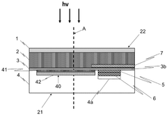
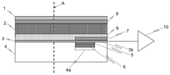
- The use of a microcavity with a reflective and semi-transparent electrode configuration, comprising a transparent conductive oxide layer and an active layer made of a blend of n-type and p-type organic semiconductors, where the active layer has high transmittance at the resonance wavelength, allowing for a narrow spectral response and high external quantum efficiency without the need for optical filters, and the resonance wavelength is tuned by adjusting the thickness of the transparent conductive oxide layer.
Photodetector, image sensor and photodetection method
PatentWO2025214971A1
Innovation
- A photodetector design incorporating a semiconductor layer, charge transfer layer, and substrate with a two-dimensional semiconductor, utilizing transparent conductive oxides and quantum dots for efficient charge carrier extraction, and a layered structure with transfer and modulation gates to control charge flow and reduce leakage.
Materials Science Advancements Enabling TCO Performance
Recent advancements in materials science have significantly enhanced the performance capabilities of Transparent Conductive Oxides (TCOs) in photodetector applications. The evolution of TCO materials has been driven by the fundamental need to balance optical transparency with electrical conductivity, a challenging trade-off that has spurred innovative approaches in materials engineering.
The development of atomic layer deposition (ALD) techniques has revolutionized TCO fabrication, enabling precise control over film thickness and composition at the nanoscale. This precision has allowed researchers to optimize the band gap engineering of materials such as indium tin oxide (ITO), fluorine-doped tin oxide (FTO), and aluminum-doped zinc oxide (AZO), resulting in enhanced carrier mobility while maintaining high optical transmittance in the visible spectrum.
Nanostructuring approaches have emerged as another critical advancement, with the introduction of TCO nanoparticles, nanowires, and nanocomposites offering increased surface area and unique optoelectronic properties. These nanostructured TCOs demonstrate superior light trapping capabilities and enhanced quantum efficiency in photodetector devices, particularly in the UV and near-IR regions where traditional TCOs often underperform.
Doping strategies have evolved beyond conventional methods, with co-doping and modulation doping techniques enabling fine-tuning of carrier concentration without compromising transparency. For instance, hydrogen-doped zinc oxide has shown remarkable improvements in conductivity while maintaining over 90% transparency across the visible spectrum, making it particularly suitable for high-performance photodetectors.
Interface engineering between TCOs and adjacent semiconductor layers has proven crucial for optimizing charge transfer and reducing recombination losses. The development of buffer layers and surface treatments has minimized band offset mismatches and reduced interface defects, significantly improving photodetector response times and sensitivity.
Flexible and stretchable TCO formulations represent another frontier, with materials science innovations enabling the deposition of high-quality TCO films on polymeric substrates. These advances have been achieved through low-temperature processing methods and the incorporation of organic-inorganic hybrid materials, opening new possibilities for wearable and conformable photodetection systems.
Computational materials science has accelerated TCO development through high-throughput screening and machine learning approaches, identifying promising new compositions and predicting their optoelectronic properties. This data-driven approach has led to the discovery of novel TCO candidates such as SrGeO₃ and BaSnO₃, which show potential for surpassing the performance limitations of traditional TCO materials in next-generation photodetector applications.
Environmental Impact and Sustainability of TCO Materials
The environmental impact of Transparent Conductive Oxide (TCO) materials in photodetector applications represents a critical consideration in the sustainable development of optoelectronic technologies. Traditional TCO materials, particularly indium tin oxide (ITO), pose significant environmental challenges due to the scarcity of indium resources. Global indium reserves are limited, with estimates suggesting potential supply constraints within the next few decades if consumption continues at current rates. This resource limitation has prompted extensive research into alternative TCO materials with reduced environmental footprints.
Manufacturing processes for TCO materials typically involve energy-intensive methods such as sputtering, chemical vapor deposition, and sol-gel techniques. These processes contribute substantially to the carbon footprint of photodetector production. Recent life cycle assessments indicate that the energy consumption during TCO deposition can account for up to 35% of the total environmental impact of photodetector manufacturing. Additionally, certain TCO production methods utilize hazardous chemicals, including strong acids and heavy metal precursors, which present waste management challenges and potential environmental contamination risks.
Emerging sustainable alternatives to conventional TCOs include aluminum-doped zinc oxide (AZO), fluorine-doped tin oxide (FTO), and carbon-based materials such as graphene and carbon nanotubes. These materials offer reduced environmental impact through more abundant constituent elements and potentially less energy-intensive production methods. For instance, AZO utilizes zinc, which is approximately 1,000 times more abundant in the Earth's crust than indium, significantly reducing resource depletion concerns.
Recycling and end-of-life management of TCO materials present both challenges and opportunities. Current recycling rates for indium from discarded electronic devices remain below 1%, representing a substantial loss of valuable resources. Improved recycling technologies, including hydrometallurgical and pyrometallurgical processes, are being developed to recover TCO materials from end-of-life photodetectors and other optoelectronic devices. These circular economy approaches could significantly reduce the environmental burden associated with TCO production.
Recent regulatory developments, including the European Union's Restriction of Hazardous Substances (RoHS) directive and the Registration, Evaluation, Authorization and Restriction of Chemicals (REACH) regulation, have increased pressure on manufacturers to adopt more environmentally benign TCO materials and production processes. These regulatory frameworks encourage the development of TCOs with reduced toxicity profiles and improved recyclability characteristics, driving innovation in sustainable photodetector technologies.
The transition toward green manufacturing techniques for TCO deposition, including low-temperature processes and reduced-energy methods such as solution processing and atmospheric pressure deposition, offers promising pathways to minimize environmental impacts while maintaining device performance. These approaches not only reduce energy consumption but also enable compatibility with flexible and biodegradable substrates, further enhancing the sustainability profile of next-generation photodetectors.
Unlock deeper insights with Patsnap Eureka Quick Research — get a full tech report to explore trends and direct your research. Try now!
Generate Your Research Report Instantly with AI Agent
Supercharge your innovation with Patsnap Eureka AI Agent Platform!
