

Transparent Conductive Oxides: Bridging Multidisciplinary Applications
OCT 27, 20259 MIN READ
Generate Your Research Report Instantly with AI Agent
Patsnap Eureka helps you evaluate technical feasibility & market potential.
TCO Technology Evolution and Objectives
Transparent Conductive Oxides (TCOs) have evolved significantly since their initial discovery in the early 20th century. The journey began with the development of tin-doped indium oxide (ITO) in the 1940s, which marked the first major milestone in TCO technology. By the 1970s, ITO had become the industry standard for applications requiring transparent electrodes, particularly in display technologies. This evolution was driven by the unique combination of optical transparency and electrical conductivity that TCOs offer, properties that were previously thought to be mutually exclusive in materials science.
The technological trajectory of TCOs has been characterized by continuous improvements in performance metrics, including higher transparency in the visible spectrum, enhanced electrical conductivity, and increased mechanical flexibility. These advancements have been achieved through refined deposition techniques, novel doping strategies, and innovative material compositions. The development of alternative TCOs such as fluorine-doped tin oxide (FTO), aluminum-doped zinc oxide (AZO), and gallium-doped zinc oxide (GZO) represents significant progress in addressing the limitations of ITO, particularly its scarcity and cost.
Recent years have witnessed a paradigm shift in TCO research, moving beyond traditional metal oxides to explore hybrid structures, nanocomposites, and organic-inorganic interfaces. This expansion has been fueled by emerging applications in flexible electronics, photovoltaics, and smart windows, each demanding specific performance characteristics that conventional TCOs struggle to provide. The integration of TCOs with other functional materials has opened new avenues for multifunctional devices that can simultaneously sense, generate energy, and display information.
The primary objective of current TCO research is to develop materials that maintain high optical transparency (>85% in the visible range) while achieving electrical conductivity comparable to metals (resistivity <10^-4 Ω·cm). Additionally, there is a growing emphasis on sustainability, seeking to replace indium-based TCOs with earth-abundant alternatives that maintain comparable performance. Mechanical flexibility has emerged as another critical goal, particularly for applications in wearable technology and flexible displays, where traditional brittle oxides face significant limitations.
Looking forward, the field aims to establish a comprehensive understanding of structure-property relationships in TCOs, enabling predictive design of materials with tailored properties for specific applications. This includes developing TCOs with selective spectral transmission, self-healing capabilities, and compatibility with large-scale, low-cost manufacturing processes. The ultimate goal is to create a versatile toolkit of TCO materials that can be precisely engineered to meet the diverse requirements of next-generation electronic and optoelectronic devices, thereby bridging multiple disciplines including materials science, physics, chemistry, and engineering.
Market Applications and Demand Analysis
The global market for Transparent Conductive Oxides (TCOs) has witnessed substantial growth, primarily driven by the expanding electronics industry and the increasing demand for touchscreen devices. The TCO market was valued at approximately $7.5 billion in 2022 and is projected to reach $12.3 billion by 2028, growing at a CAGR of 8.7% during the forecast period.
Consumer electronics represents the largest application segment for TCOs, accounting for over 40% of the total market share. The proliferation of smartphones, tablets, and other portable electronic devices has significantly contributed to this dominance. Additionally, the growing adoption of OLED displays in premium smartphones and televisions has further accelerated the demand for high-performance TCO materials.
The photovoltaic industry emerges as another crucial market for TCOs, particularly for thin-film solar cells where these materials serve as transparent electrodes. With the global push towards renewable energy sources, the solar energy sector is expected to provide substantial growth opportunities for TCO materials. Indium Tin Oxide (ITO) continues to be the most widely used TCO in solar applications, though alternatives are gaining traction due to indium's limited supply and price volatility.
Smart windows and architectural glass applications represent a rapidly growing segment for TCOs. These applications leverage the electrochromic properties of certain TCO materials to create energy-efficient building solutions. The construction industry's increasing focus on sustainable building practices has propelled the demand for smart glass technologies, with the market expected to grow at a CAGR of 12.5% through 2028.
Emerging applications in flexible electronics, wearable devices, and transparent heaters are creating new avenues for TCO materials. The healthcare sector, particularly in medical imaging and biosensors, has also begun incorporating TCO-based technologies, expanding the market potential beyond traditional applications.
Regional analysis indicates that Asia-Pacific dominates the TCO market, accounting for approximately 65% of global production and consumption. This dominance is attributed to the region's robust electronics manufacturing ecosystem, particularly in countries like China, South Korea, Japan, and Taiwan. North America and Europe follow, with significant contributions to research and development of next-generation TCO materials and applications.
The market faces challenges related to raw material supply constraints, particularly for indium-based TCOs. This has accelerated research into alternative materials such as aluminum-doped zinc oxide (AZO), fluorine-doped tin oxide (FTO), and graphene-based composites. The development of these alternatives is expected to reshape the competitive landscape of the TCO market in the coming years.
Global Research Status and Technical Barriers
Transparent Conductive Oxides (TCOs) have emerged as a critical research focus globally, with significant advancements occurring across North America, Europe, and East Asia. The United States maintains leadership in fundamental research through institutions like MIT and Stanford University, while the European Union excels in application-oriented research, particularly in photovoltaics and smart windows. East Asian countries, notably Japan, South Korea, and China, have established dominance in manufacturing scale and process optimization.
Despite these advancements, several technical barriers impede further development of TCO technologies. The trade-off between optical transparency and electrical conductivity remains a fundamental challenge, as increasing carrier concentration typically reduces transparency in the visible spectrum. This inherent contradiction limits performance in applications requiring both properties at optimal levels.
Material stability presents another significant obstacle, particularly in harsh environments or under prolonged operational conditions. TCOs often experience degradation when exposed to humidity, temperature fluctuations, or ultraviolet radiation, limiting their practical deployment in outdoor applications or devices with extended lifespans.
Manufacturing scalability constitutes a persistent barrier, with high-quality TCO films typically requiring expensive vacuum deposition techniques like sputtering or pulsed laser deposition. Solution-based methods offer cost advantages but frequently yield materials with inferior optoelectronic properties, creating a significant gap between laboratory demonstrations and commercial viability.
Interface engineering challenges also hinder TCO integration into complex device architectures. Contact resistance and band alignment issues at TCO-semiconductor interfaces can significantly degrade device performance, particularly in multilayer structures like solar cells or displays.
The environmental impact of indium-based TCOs represents a growing concern, as indium tin oxide (ITO) remains the industry standard despite indium's scarcity and extraction challenges. While alternative materials like fluorine-doped tin oxide (FTO) and aluminum-doped zinc oxide (AZO) exist, they typically underperform ITO in critical metrics.
Standardization across the industry presents additional complications, with inconsistent characterization methodologies making direct comparisons between research reports difficult. This fragmentation slows knowledge transfer and impedes collaborative progress toward solving fundamental challenges in TCO development.
Current TCO Fabrication Techniques
01 Composition and structure of transparent conductive oxides
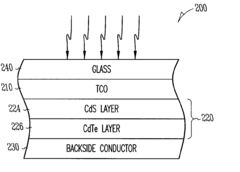
Transparent conductive oxides (TCOs) are materials that combine optical transparency with electrical conductivity. These materials typically consist of metal oxides such as indium tin oxide (ITO), zinc oxide (ZnO), or tin oxide (SnO2). The composition and crystal structure of these oxides significantly influence their electrical and optical properties. Various dopants can be incorporated to enhance conductivity while maintaining transparency in the visible spectrum.- Indium-based transparent conductive oxides: Indium-based materials, particularly indium tin oxide (ITO), are widely used as transparent conductive oxides in various electronic applications. These materials offer excellent electrical conductivity while maintaining high optical transparency in the visible spectrum. The formulation and deposition methods of indium-based TCOs can be optimized to achieve specific resistivity and transparency requirements for applications such as touch screens, displays, and photovoltaic devices.
- Alternative TCO materials to replace indium: Due to the scarcity and high cost of indium, alternative transparent conductive oxide materials are being developed. These alternatives include zinc oxide-based compounds (ZnO), tin oxide (SnO2), and other metal oxides that can be doped with various elements to enhance conductivity while maintaining transparency. These materials aim to provide comparable performance to ITO but with more abundant and cost-effective raw materials.
- Deposition and manufacturing techniques for TCOs: Various deposition techniques are employed for fabricating transparent conductive oxide films with controlled properties. These methods include sputtering, chemical vapor deposition, sol-gel processes, and atomic layer deposition. The manufacturing parameters significantly influence the crystallinity, stoichiometry, and defect structure of the TCO films, which in turn affect their electrical and optical properties. Advanced deposition techniques enable the production of TCO films with optimized performance for specific applications.
- TCO applications in optoelectronic devices: Transparent conductive oxides are crucial components in various optoelectronic devices including solar cells, light-emitting diodes, and display technologies. The integration of TCOs in these devices requires careful consideration of interface properties, work function matching, and stability under operating conditions. Specialized TCO formulations and structures are developed to meet the specific requirements of different device architectures, enhancing overall device performance and longevity.
- Nanostructured and composite TCO materials: Nanostructured and composite transparent conductive oxide materials represent an emerging approach to enhance performance beyond conventional thin films. These include nanoparticle-based TCOs, nanowire networks, and multilayer composite structures. By engineering the material at the nanoscale, properties such as conductivity, transparency, flexibility, and stability can be significantly improved. These advanced materials enable new applications in flexible electronics, smart windows, and next-generation display technologies.
02 Deposition methods for transparent conductive oxide films
Various deposition techniques are employed to create thin films of transparent conductive oxides on different substrates. These methods include sputtering, chemical vapor deposition (CVD), atomic layer deposition (ALD), sol-gel processes, and pulsed laser deposition. Each technique offers different advantages in terms of film quality, uniformity, deposition rate, and compatibility with substrate materials. The deposition parameters significantly affect the resulting film properties.Expand Specific Solutions03 Applications in optoelectronic devices
Transparent conductive oxides are widely used in various optoelectronic devices due to their unique combination of optical transparency and electrical conductivity. These applications include solar cells, light-emitting diodes (LEDs), flat panel displays, touch screens, and smart windows. In these devices, TCOs typically serve as transparent electrodes that allow light to pass through while efficiently conducting electrical current, thereby enhancing device performance and enabling new functionalities.Expand Specific Solutions04 Novel TCO materials and composites
Research on novel transparent conductive oxide materials and composites aims to overcome limitations of traditional TCOs such as indium tin oxide. These include alternative materials like aluminum-doped zinc oxide (AZO), fluorine-doped tin oxide (FTO), and various ternary compounds. Composite structures combining different TCO materials or TCOs with other materials like graphene or metal nanowires are being developed to achieve enhanced properties such as improved flexibility, lower cost, or better performance under specific conditions.Expand Specific Solutions05 Processing techniques for improved TCO performance
Various post-deposition processing techniques are employed to enhance the performance of transparent conductive oxide films. These include thermal annealing, plasma treatment, laser processing, and chemical treatments. Such processes can improve crystallinity, reduce defects, enhance carrier mobility, and optimize the trade-off between optical transparency and electrical conductivity. Advanced patterning techniques are also developed to create structured TCO films for specific applications requiring controlled optical and electrical properties.Expand Specific Solutions
Leading Manufacturers and Research Institutions
Transparent Conductive Oxides (TCOs) are currently in a growth phase, with the market expected to reach significant expansion due to increasing applications in electronics, photovoltaics, and smart technologies. The global TCO market demonstrates moderate maturity but is evolving rapidly with technological advancements. Companies like Samsung Electronics, Applied Materials, and Eastman Kodak are leading commercial development, while research institutions such as IMEC, Naval Research Laboratory, and universities including Trinity College Dublin and Peking University are advancing fundamental innovations. The technology landscape shows varying degrees of maturity across applications, with established processes for display technologies but emerging developments in flexible electronics and energy-efficient applications, creating opportunities for cross-sector collaboration between established players and research entities.
Sumitomo Metal Mining Co. Ltd.
Technical Solution: Sumitomo Metal Mining has developed advanced TCO materials focusing on indium conservation and performance enhancement. Their proprietary ITOSTAR® technology utilizes a specialized ITO composition with optimized tin doping levels (typically 5-10%) and controlled oxygen stoichiometry to achieve sheet resistance below 8 ohms/square with transparency exceeding 90%. They've pioneered indium-reduced TCO formulations incorporating zinc tin oxide (ZTO) and aluminum-doped zinc oxide (AZO) that maintain comparable performance to traditional ITO. Sumitomo's manufacturing process employs high-purity target materials (99.99%+) and advanced sputtering techniques with precise control over deposition parameters. Their TCO development includes specialized annealing processes that optimize crystallinity while minimizing defect formation. For flexible applications, they've developed composite TCO structures incorporating stress-relief layers that maintain conductivity under mechanical deformation. Sumitomo has also explored antimony-doped tin oxide (ATO) and fluorine-doped tin oxide (FTO) as specialized TCO solutions for energy applications.
Strengths: Vertically integrated supply chain from raw material mining to finished TCO products; exceptional material purity control; extensive experience in high-volume manufacturing. Weaknesses: Continued reliance on indium despite diversification efforts; traditional sputtering approaches limiting compatibility with some flexible substrates; higher cost structure compared to emerging solution-processed alternatives.
Samsung Electronics Co., Ltd.
Technical Solution: Samsung has developed advanced indium tin oxide (ITO) alternatives for flexible displays, focusing on metal-mesh and silver nanowire technologies. Their proprietary TCO formulations incorporate zinc oxide doped with aluminum (AZO) and indium-free solutions to address supply chain concerns. Samsung's approach combines atomic layer deposition (ALD) and sputtering techniques to achieve ultra-thin, highly transparent conductive layers with sheet resistance below 10 ohms/square. For foldable displays, they've pioneered hybrid TCO structures that maintain conductivity even after thousands of folding cycles, utilizing a composite structure of oxide layers and conductive polymers. Their manufacturing process enables large-area deposition with high uniformity across Gen 8+ substrates, critical for commercial display production.
Strengths: Vertical integration allowing control over entire manufacturing process; extensive IP portfolio in flexible display technologies; high-volume production capability. Weaknesses: Heavy reliance on indium-based solutions despite diversification efforts; higher production costs compared to conventional rigid display technologies.
Key Patents and Scientific Breakthroughs
Rheology-controlled conductive materials, methods of production and uses thereof
PatentInactiveUS20090035707A1
Innovation
- Compositions comprising conductive nanomaterials blended with rheology control additives, which include functionalized and unfunctionalized carbon nanotubes, semiconductor nanowires, and metal nanowires, are used to create transparent conductive materials and films that maintain high conductivity and transparency, with minimal or no surfactants, allowing for efficient application and patterning.
Atomic layer deposited titanium-doped indium oxide films
PatentActiveUS20090314345A1
Innovation
- The use of titanium-doped indium oxide films formed through atomic layer deposition (ALD) allows for controlled engineering of carrier mobility without increasing carrier concentration, thereby enhancing electrical conductivity while maintaining optical transparency.
Sustainability and Environmental Impact
The environmental impact of Transparent Conductive Oxides (TCOs) has become increasingly significant as their applications expand across multiple industries. Traditional TCO materials, particularly indium tin oxide (ITO), face sustainability challenges due to the scarcity of indium, which is classified as a critical raw material with limited global reserves. Current extraction and processing methods for these materials often involve energy-intensive processes and toxic chemicals, raising concerns about their environmental footprint throughout their lifecycle.
Manufacturing TCOs typically requires high-temperature deposition processes, consuming substantial energy and generating greenhouse gas emissions. The carbon footprint of TCO production varies significantly depending on the specific material and fabrication method employed. Recent life cycle assessments indicate that alternative TCOs such as aluminum-doped zinc oxide (AZO) and fluorine-doped tin oxide (FTO) generally demonstrate lower environmental impacts compared to conventional ITO.
Recycling and end-of-life management present additional sustainability challenges. The complex integration of TCOs into multilayer devices complicates material recovery, often resulting in valuable resources being discarded rather than reclaimed. However, emerging recycling technologies show promise in improving recovery rates of critical elements from electronic waste containing TCOs, potentially creating more circular material flows.
The development of bio-based and earth-abundant alternatives represents a promising direction for sustainable TCO innovation. Research into cellulose-based transparent conductors and carbon-based materials (graphene, carbon nanotubes) offers pathways to reduce dependence on scarce elements. These alternatives often enable lower-temperature processing, further reducing energy requirements and associated emissions.
Water consumption and pollution also merit consideration in TCO sustainability assessments. Wet chemical processes used in TCO fabrication can generate contaminated wastewater requiring treatment before discharge. Advanced manufacturing approaches incorporating green chemistry principles are being developed to minimize hazardous waste generation and water usage.
Policy frameworks increasingly influence TCO sustainability through regulations on hazardous substances, extended producer responsibility, and carbon pricing mechanisms. The European Union's Restriction of Hazardous Substances (RoHS) directive and similar global initiatives have accelerated the transition toward more environmentally benign TCO formulations and manufacturing processes.
As TCO applications continue to expand in renewable energy technologies like photovoltaics and smart windows, their net environmental impact becomes more complex to evaluate. While these applications contribute to sustainability through energy efficiency and renewable energy generation, the environmental benefits must be weighed against the impacts of TCO production and disposal to ensure genuine sustainability improvements across their complete lifecycle.
Industry Standards and Quality Control Metrics
The standardization of Transparent Conductive Oxides (TCOs) has evolved significantly over the past decade, with international bodies establishing comprehensive frameworks to ensure consistency across applications. The International Electrotechnical Commission (IEC) and American Society for Testing and Materials (ASTM) have developed specific standards for TCO materials, focusing on optical transparency, electrical conductivity, and durability parameters. These standards typically require TCOs to maintain at least 80% transparency in the visible spectrum while achieving sheet resistance below 100 Ω/sq for most commercial applications.
Quality control metrics for TCO production have become increasingly sophisticated, incorporating both in-line and post-production testing methodologies. Four-point probe measurements remain the industry standard for electrical characterization, while spectrophotometry provides critical data on optical performance across various wavelengths. Advanced facilities now implement automated optical inspection systems capable of detecting nanoscale defects that could compromise device performance.
Environmental stability testing has gained prominence in TCO quality assessment protocols, with accelerated aging tests now standard practice. These tests typically expose materials to elevated temperatures (85°C), high humidity (85% RH), and UV radiation for periods ranging from 1,000 to 2,000 hours to simulate years of operational conditions. The ITO-90 certification, established in 2018, has become a benchmark for premium-grade TCOs, requiring less than 5% degradation in conductivity after 1,000 hours of environmental stress testing.
Manufacturing tolerance specifications have tightened considerably, with thickness uniformity requirements now typically ±2% across 300mm substrates. Leading manufacturers implement statistical process control (SPC) methodologies to monitor critical parameters in real-time, with six-sigma quality targets becoming the industry norm for high-end applications in optoelectronics and photovoltaics.
The emergence of application-specific standards represents a significant trend, with distinct certification pathways for TCOs intended for different sectors. The SEMI PV211 standard addresses requirements for photovoltaic applications, while the Display Technology Committee's DTC-75 protocol establishes benchmarks for touch-panel implementations. These specialized frameworks acknowledge the diverse performance requirements across applications, from flexibility needs in wearable electronics to extreme durability in architectural glazing.
Harmonization efforts between regional standards bodies have accelerated, with the International TCO Consortium (ITCOC) facilitating alignment between Asian, European, and North American certification systems. This convergence has simplified compliance for global manufacturers while establishing more consistent quality expectations across international markets.
Unlock deeper insights with Patsnap Eureka Quick Research — get a full tech report to explore trends and direct your research. Try now!
Generate Your Research Report Instantly with AI Agent
Supercharge your innovation with Patsnap Eureka AI Agent Platform!