Comparison of Transparent Conductive Oxides vs Traditional Semiconductors
OCT 27, 20259 MIN READ
Generate Your Research Report Instantly with AI Agent
Patsnap Eureka helps you evaluate technical feasibility & market potential.
TCO Evolution and Research Objectives
Transparent Conductive Oxides (TCOs) have emerged as a revolutionary class of materials in the field of optoelectronics over the past several decades. The evolution of TCOs began in the early 20th century with the discovery of cadmium oxide's conductive properties, but significant advancements only materialized in the 1970s with the development of indium tin oxide (ITO). This material became the industry standard due to its exceptional combination of optical transparency and electrical conductivity, properties that are typically mutually exclusive in traditional semiconductors.
The technological trajectory of TCOs has been driven by increasing demands in display technologies, photovoltaics, and smart windows. While traditional semiconductors like silicon and gallium arsenide have dominated the electronics industry, their opacity limits applications requiring both conductivity and transparency. This fundamental limitation created the research space that TCOs now occupy, offering a unique solution to this materials science paradox.
Recent years have witnessed an acceleration in TCO research, particularly focused on addressing the scarcity and cost issues associated with indium-based compounds. Alternative TCOs such as aluminum-doped zinc oxide (AZO), fluorine-doped tin oxide (FTO), and more recently, amorphous oxide semiconductors like indium-gallium-zinc oxide (IGZO) represent significant milestones in this evolution. Each iteration has aimed to optimize the delicate balance between transparency, conductivity, and manufacturing feasibility.
The primary objective of current TCO research is to develop materials that can match or exceed ITO's performance while eliminating its drawbacks. Specifically, researchers aim to discover compositions that offer higher electron mobility, greater optical transparency across broader wavelength ranges, enhanced mechanical flexibility, and improved stability under various environmental conditions. Additionally, there is a strong focus on developing TCOs from earth-abundant elements to ensure sustainability and cost-effectiveness.
Another critical research goal involves understanding the fundamental physics and chemistry governing the seemingly contradictory properties of TCOs. While traditional semiconductors operate based on well-established band theory, the mechanisms enabling simultaneous transparency and conductivity in TCOs involve more complex phenomena including defect chemistry and band structure engineering. Elucidating these mechanisms will facilitate more rational design approaches for next-generation TCOs.
Looking forward, the research trajectory aims to bridge the performance gap between TCOs and traditional semiconductors in terms of carrier mobility and stability, while maintaining the unique transparency advantage. This convergence would enable entirely new device architectures and applications, potentially revolutionizing fields from renewable energy to consumer electronics.
Market Analysis for Transparent Electronics
The transparent electronics market has witnessed substantial growth in recent years, driven primarily by increasing demand for advanced display technologies and smart devices. Currently valued at approximately $3.2 billion, the market is projected to reach $7.5 billion by 2027, representing a compound annual growth rate (CAGR) of 18.7%. This remarkable growth trajectory is fueled by expanding applications across consumer electronics, automotive displays, and emerging smart architectural solutions.
Consumer electronics remains the dominant segment, accounting for nearly 45% of the total market share. Smartphones and tablets utilizing transparent conductive materials have seen particularly strong adoption rates, with major manufacturers increasingly incorporating these technologies into flagship products. The automotive sector represents the fastest-growing application area, with a projected CAGR of 22.3% through 2027, as heads-up displays and smart windshields gain traction.
Geographically, Asia-Pacific leads the market with approximately 52% share, driven by the concentration of electronics manufacturing facilities and display production in countries like South Korea, Japan, China, and Taiwan. North America and Europe follow with 24% and 19% market shares respectively, with significant research activities and premium consumer adoption rates.
The transparent electronics value chain encompasses raw material suppliers, component manufacturers, device integrators, and end-product companies. Indium tin oxide (ITO) currently dominates the transparent conductive materials segment with approximately 78% market share, though alternative materials like silver nanowires, graphene, and metal mesh are gaining momentum due to ITO's supply constraints and brittleness limitations.
Key market drivers include the growing demand for flexible and foldable displays, increasing adoption of touch-enabled interfaces across multiple industries, and the emergence of Internet of Things (IoT) applications requiring transparent sensing components. The push toward energy efficiency has also bolstered interest in smart windows and photovoltaic applications utilizing transparent electronics.
Market challenges include high production costs, technical limitations in achieving optimal combinations of transparency and conductivity, and material sustainability concerns. The limited availability of indium, a key component in ITO, has prompted significant research into alternative materials, creating both challenges and opportunities for market participants.
TCO vs Semiconductor Technical Challenges
Transparent Conductive Oxides (TCOs) and traditional semiconductors present distinct technical challenges that significantly impact their applications and performance characteristics. TCOs face fundamental limitations in achieving simultaneously high optical transparency and electrical conductivity due to their inherent material properties. The carrier concentration in TCOs typically needs to exceed 10^20 cm^-3 to achieve acceptable conductivity, which often compromises transparency in the visible spectrum. This trade-off represents a persistent challenge that researchers continue to address through various doping strategies and material engineering approaches.
Traditional semiconductors, conversely, excel in electrical performance but struggle with transparency issues. Silicon, gallium arsenide, and other conventional semiconductors possess band gaps that absorb visible light, making them inherently opaque. While thinning these materials can improve transparency, this approach significantly compromises their electrical properties and mechanical stability, limiting practical applications where both visibility and conductivity are required.
Manufacturing scalability presents another significant challenge. TCOs like ITO (Indium Tin Oxide) require specialized deposition techniques such as sputtering or chemical vapor deposition to achieve uniform thin films with optimal properties. The scarcity of indium has driven research toward alternative TCOs, yet these alternatives often exhibit inferior performance characteristics. Traditional semiconductors benefit from decades of manufacturing optimization but require complex and expensive clean room facilities for high-quality production.
Stability and durability under operating conditions diverge significantly between these materials. TCOs frequently demonstrate degradation when exposed to elevated temperatures, humidity, or mechanical stress. This degradation manifests as increased resistivity and reduced transparency over time. Traditional semiconductors generally offer superior thermal stability but may require extensive encapsulation to protect against environmental factors, adding complexity to device architecture.
Interface engineering represents a critical challenge for both material systems. TCOs must form effective electrical contacts with adjacent layers while maintaining transparency at these interfaces. Traditional semiconductors require careful band alignment and contact engineering to minimize resistance and prevent carrier recombination. The formation of stable, low-resistance contacts without compromising other performance metrics remains technically demanding for both material classes.
Flexibility requirements in modern electronics pose additional challenges. TCOs typically exhibit brittle behavior when deposited on flexible substrates, leading to crack formation and conductivity loss during bending. While traditional semiconductors can be processed into flexible formats through techniques like transfer printing or the use of organic semiconductors, these approaches often compromise performance or increase manufacturing complexity significantly.
Current TCO Implementation Approaches
01 Transparent Conductive Oxide Materials and Compositions
Transparent conductive oxides (TCOs) are materials that combine electrical conductivity with optical transparency. These materials typically include indium tin oxide (ITO), zinc oxide (ZnO), and other metal oxides that can be doped to enhance conductivity while maintaining transparency. The composition and structure of these materials are critical for their performance in various applications such as displays, solar cells, and touch screens.- Transparent Conductive Oxide Compositions and Fabrication Methods: Various compositions of transparent conductive oxides (TCOs) are used in electronic and optoelectronic devices. These materials combine optical transparency with electrical conductivity, making them suitable for applications such as displays, solar cells, and touch screens. Fabrication methods include sputtering, chemical vapor deposition, and sol-gel processes to achieve desired electrical and optical properties. Common TCO materials include indium tin oxide (ITO), zinc oxide, and tin oxide doped with various elements to enhance conductivity while maintaining transparency.
- Integration of TCOs with Traditional Semiconductors: The integration of transparent conductive oxides with traditional semiconductor materials creates hybrid devices with enhanced functionality. This combination allows for the development of novel electronic components that benefit from both the transparency of TCOs and the well-established electronic properties of conventional semiconductors. Applications include thin-film transistors, heterojunction solar cells, and advanced display technologies. The interface between TCOs and semiconductors requires careful engineering to minimize defects and optimize charge transfer.
- TCO-based Display and Touch Screen Technologies: Transparent conductive oxides are essential components in modern display and touch screen technologies. These materials form transparent electrodes that allow light to pass through while conducting electrical signals. The development of flexible, durable, and highly responsive touch screens relies on advanced TCO formulations with optimized sheet resistance and optical transparency. Innovations in this area focus on reducing material costs, improving durability, and enhancing touch sensitivity for various consumer electronic devices.
- TCO Applications in Photovoltaic Devices: Transparent conductive oxides play a crucial role in photovoltaic devices as transparent electrodes that allow sunlight to reach the active semiconductor layers while collecting generated charge carriers. The development of TCOs with high transparency in the visible spectrum, low sheet resistance, and good stability has significantly improved solar cell efficiency. Research focuses on cost-effective TCO materials that can replace expensive indium-based compounds while maintaining performance in various types of solar cells, including thin-film, perovskite, and heterojunction architectures.
- Novel TCO Materials and Surface Modifications: Research on novel transparent conductive oxide materials and surface modifications aims to overcome limitations of traditional TCOs. This includes developing indium-free alternatives to address the scarcity and cost of indium, enhancing electrical conductivity without sacrificing optical transparency, and improving stability under various environmental conditions. Surface modifications through plasma treatment, chemical functionalization, or nanostructuring can enhance TCO performance for specific applications. These innovations enable TCOs to meet the demanding requirements of next-generation electronic and optoelectronic devices.
02 Fabrication Methods for Transparent Conductive Films
Various deposition and processing techniques are employed to create transparent conductive films. These methods include sputtering, chemical vapor deposition, sol-gel processes, and printing techniques. The fabrication parameters significantly influence the film's properties, including transparency, conductivity, and durability. Post-deposition treatments such as annealing can further enhance the performance characteristics of these films.Expand Specific Solutions03 Integration of TCOs with Traditional Semiconductors
The integration of transparent conductive oxides with traditional semiconductor materials creates hybrid structures with enhanced functionality. These combinations enable the development of novel electronic and optoelectronic devices. The interface between TCOs and semiconductors requires careful engineering to manage band alignment, minimize defects, and optimize charge transfer. Such integration is crucial for applications in thin-film transistors, photovoltaics, and sensors.Expand Specific Solutions04 Applications in Display and Touchscreen Technologies
Transparent conductive oxides play a vital role in display and touchscreen technologies. They serve as transparent electrodes in liquid crystal displays, organic light-emitting diodes, and capacitive touch panels. The combination of optical transparency and electrical conductivity makes these materials ideal for applications where visible light must pass through while maintaining electrical functionality. Advancements in TCO technology have enabled the development of flexible, high-resolution displays and responsive touch interfaces.Expand Specific Solutions05 Novel TCO Formulations and Performance Enhancements
Research in transparent conductive oxides focuses on developing new formulations with improved properties. These innovations include nanostructured TCOs, composite materials, and alternative dopants that enhance conductivity without sacrificing transparency. Efforts are also directed toward creating more environmentally friendly alternatives to indium-based TCOs, addressing concerns about indium scarcity and cost. These novel formulations aim to achieve higher conductivity, better transparency, improved flexibility, and enhanced stability under various environmental conditions.Expand Specific Solutions
Industry Leaders and Competitive Landscape
Transparent Conductive Oxides (TCOs) versus traditional semiconductors represents a dynamic competitive landscape in the optoelectronics industry. Currently in a growth phase, the TCO market is expanding at approximately 6-8% annually, driven by increasing demand for touchscreens, displays, and photovoltaics. While traditional semiconductors (represented by Samsung Electronics, Texas Instruments, and SK Hynix) maintain dominance in computing applications, TCOs are gaining traction in specialized applications requiring optical transparency with electrical conductivity. Companies like Samsung Display, LG Display, and OSRAM are leading TCO innovation, particularly for display technologies. Academic institutions including Oregon State University and Northwestern University are advancing fundamental research, while Semiconductor Energy Laboratory and Powerchip are developing hybrid technologies that bridge both material systems, suggesting future convergence of these technologies in next-generation electronic devices.
Semiconductor Energy Laboratory Co., Ltd.
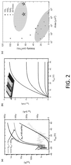
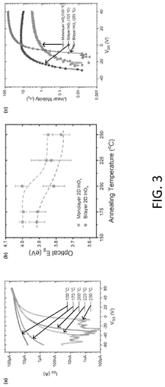
Technical Solution: Semiconductor Energy Laboratory (SEL) has developed advanced oxide semiconductor technology, particularly focusing on IGZO (Indium Gallium Zinc Oxide) as a transparent conductive oxide material. Their approach combines IGZO with conventional silicon-based semiconductors to create hybrid devices with enhanced performance characteristics. SEL's technology enables the fabrication of transparent thin-film transistors (TFTs) with electron mobility exceeding 10 cm²/Vs, significantly higher than amorphous silicon (a-Si) at approximately 0.5-1 cm²/Vs. Their proprietary c-axis aligned crystalline IGZO (CAAC-IGZO) technology demonstrates remarkable stability under various environmental conditions, including temperature fluctuations and light exposure, while maintaining transparency above 80% in the visible spectrum. SEL has successfully implemented these materials in display applications, achieving lower power consumption through reduced leakage current (approximately 10^-24 A/μm) compared to conventional semiconductors, and enabling higher resolution displays with smaller transistor sizes.
Strengths: Superior electron mobility compared to a-Si while maintaining transparency; exceptional stability under environmental stressors; ultra-low leakage current enabling power-efficient devices; compatibility with existing manufacturing infrastructure. Weaknesses: Higher production costs compared to traditional semiconductors; limited high-frequency performance compared to crystalline silicon; requires specialized deposition techniques to achieve optimal performance.
Samsung Electronics Co., Ltd.
Technical Solution: Samsung Electronics has developed comprehensive TCO (Transparent Conductive Oxide) technologies that integrate with their semiconductor expertise. Their approach focuses on oxide semiconductor thin-film transistors (TFTs) using indium gallium zinc oxide (IGZO) and zinc oxide (ZnO) variants. Samsung's proprietary metal oxide TFT technology achieves electron mobility of 15-30 cm²/Vs while maintaining transparency above 80%, significantly outperforming traditional amorphous silicon semiconductors. Their advanced TCO electrodes demonstrate sheet resistance below 10 ohms/square with optical transmittance exceeding 90% in the visible spectrum. Samsung has implemented these materials in their Quantum Dot OLED displays, enabling pixel densities above 1000 PPI with aperture ratios exceeding 60%, impossible with conventional silicon-based backplanes. Their manufacturing process incorporates low-temperature deposition techniques (below 350°C), allowing compatibility with flexible substrates and enabling their curved and foldable display technologies. Recent developments include doped ZnO systems that reduce dependence on indium while maintaining comparable electrical performance and optical properties.
Strengths: Vertical integration capabilities from materials research to device manufacturing; established high-volume production infrastructure; successful commercialization across multiple product categories; advanced implementation in flexible display technologies. Weaknesses: Complex manufacturing processes requiring precise control of oxygen vacancies; challenges in long-term stability under high current conditions; higher initial production costs compared to traditional semiconductor technologies.
Key Patents and Scientific Breakthroughs
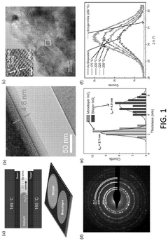
Transparent conductive oxide thin film substrate, method of fabricating the same, and organic light-emitting device and photovoltaic cell having the same
PatentActiveEP2690683A3
Innovation
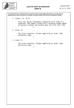
- A bi-layer transparent conductive oxide thin film substrate is fabricated using a base substrate with a first transparent conductive oxide thin film treated with a low concentration dopant, followed by a second thin film treated with a higher concentration dopant, achieving a smoother surface and reduced leakage current, and the process includes an inner and outer light extraction layer for enhanced performance.
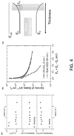
Liquid metal printed 2d ultrahigh mobility conducting oxide transistors
PatentPendingUS20240332017A1
Innovation
- A liquid metal printing method that operates at low temperatures (40° C to 450° C) to form alloyed oxide films, enabling the deposition of nanocrystalline ultrathin films with high conductivity and transparency, suitable for large-area flexible electronics, by using a dielectric and metal workpieces to form an alloyed oxide film with precise control over thickness and electronic properties.
Materials Sustainability Assessment
The sustainability assessment of materials used in transparent conductive oxides (TCOs) versus traditional semiconductors reveals significant environmental and economic implications for the electronics industry. TCOs, primarily composed of indium tin oxide (ITO), zinc oxide (ZnO), and fluorine-doped tin oxide (FTO), generally demonstrate lower environmental footprints compared to traditional semiconductor materials like silicon, gallium arsenide, and germanium.
Raw material extraction for TCOs, particularly indium, presents sustainability challenges due to its scarcity and concentration in specific geographical regions. Indium is primarily obtained as a byproduct of zinc mining, with China controlling approximately 50% of global production. This concentration creates supply chain vulnerabilities and potential price volatility. However, newer TCO alternatives utilizing more abundant elements like zinc and tin offer promising pathways toward reduced resource dependency.
Manufacturing processes for TCOs typically require lower energy inputs compared to traditional semiconductors. While silicon wafer production demands temperatures exceeding 1400°C, many TCO deposition techniques operate at substantially lower temperatures (200-400°C). This temperature differential translates to approximately 30-40% energy savings during manufacturing, significantly reducing carbon emissions throughout the production lifecycle.
End-of-life considerations strongly favor TCOs over traditional semiconductors. Most TCO materials can be recycled with recovery rates of 60-80%, whereas complex semiconductor compounds often achieve only 20-35% recovery rates. Additionally, TCOs generally contain fewer toxic elements than compound semiconductors like gallium arsenide, which require specialized handling during disposal to prevent environmental contamination.
Lifecycle assessment studies indicate that TCO-based devices typically generate 25-40% less carbon equivalent emissions compared to traditional semiconductor alternatives when evaluated across their complete lifecycle. This advantage stems primarily from lower processing temperatures, reduced material complexity, and improved recyclability profiles.
Economic sustainability metrics reveal that while traditional semiconductors currently maintain cost advantages in high-performance applications, TCOs demonstrate superior cost-effectiveness in large-area applications like displays and photovoltaics. The price volatility of indium remains a concern, with historical fluctuations exceeding 300% within five-year periods, driving research toward more abundant alternative materials.
Water usage represents another critical sustainability metric, with traditional semiconductor fabrication consuming 2,000-5,000 liters per square meter of processed material, while TCO production typically requires 40-60% less water. This difference becomes increasingly significant as water scarcity affects more manufacturing regions globally.
Manufacturing Scalability Analysis
The manufacturing scalability of Transparent Conductive Oxides (TCOs) represents a significant advantage over traditional semiconductors in various applications. TCOs such as Indium Tin Oxide (ITO), Fluorine-doped Tin Oxide (FTO), and Aluminum-doped Zinc Oxide (AZO) can be deposited using established large-area coating techniques including sputtering, chemical vapor deposition, and sol-gel processes. These methods enable cost-effective production on substrates measuring several square meters, making TCOs particularly suitable for applications like flat panel displays, photovoltaics, and smart windows.
Traditional semiconductors, while offering superior electronic properties, typically require more complex manufacturing processes involving high-temperature epitaxial growth, ion implantation, and multiple lithography steps. These processes are inherently more expensive and limited to smaller substrate sizes, typically measured in inches rather than meters. The requirement for ultra-high purity and crystalline perfection further increases production costs and reduces yield rates.
The temperature sensitivity of manufacturing processes creates another notable distinction. Many TCOs can be deposited at relatively low temperatures (below 200°C), enabling compatibility with temperature-sensitive substrates such as polymers and flexible materials. In contrast, traditional semiconductor processing often requires temperatures exceeding 1000°C, limiting substrate options and increasing energy consumption and production costs.
Equipment investment represents another critical factor in manufacturing scalability. TCO production facilities typically require lower capital expenditure compared to semiconductor fabs, which can cost billions of dollars to establish. This lower barrier to entry has enabled more diverse market participation in TCO production, though quality consistency remains a challenge for some manufacturers.
Supply chain considerations also impact scalability. Some TCOs, particularly ITO, face raw material constraints due to limited indium reserves, prompting research into alternative materials. Traditional semiconductors primarily use silicon, which is abundant, though ultra-high purity silicon production has its own supply chain complexities.
Recent advancements in roll-to-roll processing for TCOs have further enhanced their manufacturing advantage for large-area applications. This continuous production method significantly reduces per-unit costs and enables integration with flexible electronics manufacturing. Traditional semiconductors remain largely confined to batch processing paradigms, though innovations in printed electronics are beginning to bridge this gap for specific applications.
Unlock deeper insights with Patsnap Eureka Quick Research — get a full tech report to explore trends and direct your research. Try now!
Generate Your Research Report Instantly with AI Agent
Supercharge your innovation with Patsnap Eureka AI Agent Platform!