Transparent Conductive Oxides' Role in Photonic Device Integration
OCT 27, 20259 MIN READ
Generate Your Research Report Instantly with AI Agent
Patsnap Eureka helps you evaluate technical feasibility & market potential.
TCO Technology Background and Objectives
Transparent Conductive Oxides (TCOs) have emerged as critical materials in modern optoelectronic and photonic technologies, evolving from simple transparent electrodes to multifunctional components in integrated photonic devices. The development of TCOs began in the 1970s with indium tin oxide (ITO) applications in display technologies, but their role has expanded dramatically with the advancement of nanophotonics and integrated photonics over the past two decades.
The technological evolution of TCOs has been driven by the increasing demand for materials that combine optical transparency with electrical conductivity—properties that are fundamentally contradictory in conventional materials. This unique combination makes TCOs indispensable in applications ranging from solar cells and flat-panel displays to emerging fields like silicon photonics, metamaterials, and quantum photonic circuits.
Recent advancements in deposition techniques, including atomic layer deposition (ALD), pulsed laser deposition (PLD), and RF magnetron sputtering, have enabled precise control over TCO film properties at the nanoscale. This has facilitated the integration of TCOs with conventional semiconductor platforms, opening new possibilities for hybrid photonic devices with enhanced functionality.
The primary technical objective in TCO development for photonic integration is achieving optimal balance between optical transparency in target wavelength ranges (typically visible to near-infrared) and electrical conductivity. Secondary objectives include enhancing material compatibility with existing semiconductor fabrication processes, improving thermal stability, and reducing manufacturing costs through alternative material compositions that decrease reliance on scarce elements like indium.
Current research is particularly focused on developing TCOs with tunable optical properties, including actively controllable refractive indices and plasmonic responses. These developments aim to enable dynamic photonic components such as modulators, switches, and reconfigurable metasurfaces that can be integrated into complex photonic circuits.
The integration of TCOs in photonic devices represents a convergence of materials science, optics, and electronics, with the potential to address key challenges in information technology, sensing, and energy conversion. As photonic integration continues to advance toward higher densities and more complex functionalities, TCOs are expected to play an increasingly vital role in bridging the gap between electronic and photonic domains.
Looking forward, the technological trajectory of TCOs in photonic integration is moving toward atomically engineered multilayer structures, doping strategies for precise property control, and novel compositions beyond traditional indium-based materials, with particular emphasis on environmentally sustainable alternatives like aluminum-doped zinc oxide (AZO) and fluorine-doped tin oxide (FTO).
Market Analysis for Photonic Integrated Devices
The global market for photonic integrated devices is experiencing robust growth, driven by increasing demand for high-speed data transmission, telecommunications infrastructure, and advanced sensing applications. Current market valuations place the photonic integrated circuit (PIC) sector at approximately 1.3 billion USD in 2023, with projections indicating a compound annual growth rate of 23% through 2030, potentially reaching 5.5 billion USD by the end of the decade.
Transparent Conductive Oxides (TCOs) represent a critical component within this expanding market, serving as essential materials for enabling efficient light manipulation, modulation, and detection in integrated photonic devices. The TCO segment within photonics is growing at nearly 18% annually, outpacing several other material categories due to its versatility and performance characteristics.
Geographically, North America currently leads the photonic integration market with approximately 38% market share, followed by Europe (27%) and Asia-Pacific (25%). However, the Asia-Pacific region demonstrates the fastest growth trajectory, with China and Taiwan making significant investments in photonic manufacturing infrastructure. This regional shift is reshaping supply chains and technology development centers globally.
Application-wise, data communications remains the dominant sector, accounting for 42% of the photonic integrated device market. However, emerging applications in quantum computing, LiDAR systems for autonomous vehicles, and biomedical sensing are expanding rapidly, with collective growth rates exceeding 30% annually. TCO-based devices are particularly well-positioned in these emerging sectors due to their unique electro-optical properties.
Consumer demand trends indicate increasing preference for smaller, more energy-efficient devices with enhanced functionality. This directly benefits TCO-based photonic solutions, which offer superior performance-to-size ratios compared to traditional electronic components. Market research indicates that devices incorporating advanced TCO materials command premium pricing, with margins 15-20% higher than conventional alternatives.
Competitive analysis reveals a market structure transitioning from fragmentation toward consolidation, with several major acquisitions occurring in the past 24 months. Established telecommunications equipment manufacturers are actively acquiring specialized photonic integration startups, particularly those with proprietary TCO implementation technologies. This consolidation trend is expected to continue as the technology matures and commercial applications expand beyond current limitations.
TCO Development Status and Technical Barriers
Transparent Conductive Oxides (TCOs) have emerged as critical materials in photonic device integration, with significant advancements achieved over the past decade. Currently, the most widely deployed TCO materials include Indium Tin Oxide (ITO), Aluminum-doped Zinc Oxide (AZO), and Fluorine-doped Tin Oxide (FTO). ITO dominates the market with approximately 60% share due to its excellent combination of optical transparency (>90% in visible spectrum) and electrical conductivity (resistivity as low as 1×10^-4 Ω·cm).
Despite these achievements, TCO integration in photonic devices faces several significant technical barriers. Material compatibility issues arise when incorporating TCOs with other semiconductor platforms, particularly silicon photonics and III-V compound semiconductors. The thermal budget mismatch between TCO deposition processes (typically requiring 200-400°C) and temperature-sensitive photonic components often results in performance degradation of the integrated system.
Deposition uniformity presents another major challenge, especially for large-area applications and complex 3D photonic structures. Current techniques struggle to maintain consistent thickness and electrical properties across varied topographies, with thickness variations typically exceeding ±5% across 300mm wafers. This non-uniformity directly impacts device performance consistency and manufacturing yield.
Interface quality between TCOs and adjacent materials significantly affects device performance. High contact resistance and poor adhesion at these interfaces can lead to reliability issues and reduced device efficiency. Current TCO-semiconductor interfaces typically exhibit specific contact resistances in the range of 10^-5 to 10^-3 Ω·cm², which remains suboptimal for high-performance photonic applications.
Long-term stability poses another critical barrier, as TCO properties can degrade under operational conditions. Environmental factors such as humidity, temperature cycling, and prolonged light exposure can alter TCO transparency and conductivity over time. Studies indicate that some TCO materials can lose up to 15% of their initial conductivity after 1000 hours of operation under standard conditions.
The trade-off between optical transparency and electrical conductivity remains a fundamental challenge. As conductivity increases through higher doping levels, optical absorption typically increases as well, particularly in the near-infrared region critical for many photonic applications. This inverse relationship limits the performance envelope of current TCO materials.
Cost and sustainability concerns also present significant barriers to widespread adoption. The reliance on scarce elements like indium in ITO raises supply chain vulnerabilities, with indium prices fluctuating by over 300% in the past decade. Additionally, environmentally friendly deposition methods that reduce energy consumption and toxic precursors remain underdeveloped for high-performance TCO integration.
Current TCO Implementation Approaches
01 Indium-based transparent conductive oxides
Indium-based materials, particularly indium tin oxide (ITO), are widely used as transparent conductive oxides in various electronic applications. These materials offer excellent electrical conductivity while maintaining high optical transparency in the visible spectrum. Research focuses on improving deposition methods, reducing indium content due to its scarcity, and enhancing performance characteristics such as conductivity and transparency for applications in displays, touch panels, and photovoltaic devices.- Indium-based transparent conductive oxides: Indium-based materials, particularly indium tin oxide (ITO), are widely used as transparent conductive oxides in various electronic applications. These materials offer excellent electrical conductivity while maintaining high optical transparency in the visible spectrum. The formulation and deposition methods of indium-based TCOs can be optimized to achieve specific resistivity and transparency requirements for applications such as touch screens, displays, and photovoltaic devices.
- Alternative TCO materials to replace indium: Due to the scarcity and high cost of indium, alternative transparent conductive oxide materials are being developed. These include zinc oxide-based compounds (ZnO), often doped with aluminum, gallium or other elements, as well as tin oxide-based materials. These alternative TCOs aim to provide comparable electrical and optical properties to ITO while reducing dependency on rare elements and lowering manufacturing costs for electronic devices.
- Deposition and manufacturing techniques for TCOs: Various deposition techniques are employed to create transparent conductive oxide thin films with optimal properties. These include sputtering, chemical vapor deposition, sol-gel processes, and atomic layer deposition. The manufacturing parameters such as temperature, pressure, and gas composition significantly influence the crystallinity, conductivity, and transparency of the resulting TCO films. Advanced techniques focus on achieving uniform films with low resistivity at reduced processing temperatures.
- TCO applications in optoelectronic devices: Transparent conductive oxides are crucial components in various optoelectronic devices including solar cells, light-emitting diodes, and display technologies. The specific requirements for TCOs vary depending on the application, with solar cells requiring high transparency in specific wavelength ranges and displays needing precise control of optical and electrical properties. Recent developments focus on enhancing device efficiency through improved TCO performance and integration with other device components.
- Nanostructured and composite TCO materials: Nanostructured transparent conductive oxides and composite materials represent an emerging area of research aimed at enhancing both electrical and optical properties beyond conventional TCO limitations. These include nanoparticle-based films, nanowire networks, and multilayer structures combining different TCO materials. Such advanced structures can provide benefits like increased surface area, improved flexibility, and enhanced light trapping capabilities, making them particularly valuable for next-generation flexible electronics and high-efficiency photovoltaics.
02 Zinc oxide-based transparent conductive materials
Zinc oxide (ZnO) based transparent conductive materials represent an important alternative to indium-based TCOs. These materials are typically doped with elements such as aluminum, gallium or indium to enhance conductivity while maintaining transparency. ZnO-based TCOs offer advantages including abundance of raw materials, lower cost, and environmental friendliness. They can be deposited using various techniques including sputtering, chemical vapor deposition, and solution-based methods for applications in thin-film solar cells, LEDs, and flexible electronics.Expand Specific Solutions03 Fabrication methods for transparent conductive oxide films
Various fabrication methods are employed to produce high-quality transparent conductive oxide films with optimized properties. These include physical vapor deposition techniques such as sputtering and evaporation, chemical vapor deposition, sol-gel processes, and solution-based deposition methods. Each technique offers different advantages in terms of film quality, process temperature, scalability, and cost-effectiveness. Recent innovations focus on low-temperature processes compatible with flexible substrates and methods to achieve precise control over film thickness, crystallinity, and interface properties.Expand Specific Solutions04 Novel transparent conductive oxide compositions and structures
Research on novel transparent conductive oxide compositions focuses on developing materials with improved performance characteristics and reduced reliance on scarce elements. This includes multicomponent oxides, composite structures, and nanostructured materials. These novel compositions aim to achieve higher conductivity, better transparency, improved stability, and enhanced flexibility compared to conventional TCOs. Approaches include developing ternary and quaternary oxide systems, creating multilayer structures, and incorporating nanoparticles or nanowires to enhance specific properties for next-generation electronic and optoelectronic devices.Expand Specific Solutions05 Applications of transparent conductive oxides in electronic devices
Transparent conductive oxides find applications in a wide range of electronic and optoelectronic devices. They serve as transparent electrodes in displays, touchscreens, solar cells, smart windows, and organic light-emitting diodes. The specific requirements for TCOs vary depending on the application, with some prioritizing conductivity while others emphasize transparency, flexibility, or stability. Recent developments focus on integrating TCOs into flexible and wearable electronics, enhancing their compatibility with organic materials, and improving their performance in energy harvesting and storage devices.Expand Specific Solutions
Leading Companies in TCO and Photonic Integration
Transparent Conductive Oxides (TCOs) are currently in a growth phase within photonic device integration, with the market expected to expand significantly due to increasing demand for advanced optoelectronic applications. The technology demonstrates moderate maturity, with established players like Samsung Electronics, AGC, and Corning leading commercial development while research institutions such as ICFO and Industrial Technology Research Institute drive innovation. Emerging companies like Ubiquitous Energy are pioneering novel applications in transparent solar technologies. The competitive landscape features a mix of large materials manufacturers, specialized technology firms, and academic institutions collaborating to overcome challenges in balancing optical transparency with electrical conductivity for next-generation photonic devices.
Samsung Electronics Co., Ltd.
Technical Solution: Samsung has developed advanced Transparent Conductive Oxide (TCO) materials, particularly focusing on Indium Tin Oxide (ITO) alternatives for their display technologies. Their approach involves using amorphous Indium Zinc Oxide (a-IZO) and Indium Gallium Zinc Oxide (IGZO) thin films that offer superior electron mobility and optical transparency. Samsung's TCO implementation enables the integration of transparent electrodes in OLED displays, touchscreens, and emerging photonic devices. Their proprietary deposition techniques achieve sheet resistance below 10 ohms/square while maintaining over 90% optical transparency in the visible spectrum. Samsung has also pioneered the use of ultra-thin TCO layers (under 100nm) that minimize optical losses while maintaining electrical conductivity, crucial for high-efficiency photonic devices. Their recent developments include flexible TCO formulations compatible with bendable and foldable display technologies, addressing one of the key limitations of traditional brittle oxide materials.
Strengths: Samsung's TCO technologies offer exceptional balance between transparency and conductivity, with industry-leading thin film uniformity across large substrates. Their manufacturing infrastructure enables cost-effective mass production. Weaknesses: Their proprietary TCO formulations often require specialized deposition equipment, limiting broader adoption outside Samsung's ecosystem. Some of their advanced TCO materials rely on rare earth elements, raising sustainability concerns.
Sumitomo Metal Mining Co. Ltd.
Technical Solution: Sumitomo Metal Mining has developed specialized TCO materials focused on high-performance applications in photonic devices. Their flagship technology centers on ATO (Antimony-doped Tin Oxide) and FTO (Fluorine-doped Tin Oxide) formulations that offer exceptional thermal stability up to 600°C, making them suitable for high-temperature photonic applications where traditional ITO would degrade. Sumitomo's proprietary sputtering and sol-gel deposition techniques enable precise control of film thickness and composition, achieving sheet resistance as low as 8 ohms/square with transparency exceeding 85% across the visible and near-infrared spectrum. Their TCO materials feature engineered surface morphology that enhances light trapping in photovoltaic applications, improving overall device efficiency. Sumitomo has also pioneered nanocomposite TCO structures that incorporate silver nanowires within oxide matrices, creating hybrid materials with enhanced conductivity while maintaining optical transparency. Their recent innovations include TCO materials specifically designed for integration with silicon photonics platforms, featuring tailored refractive indices to minimize coupling losses at interfaces.
Strengths: Sumitomo's TCO materials demonstrate exceptional thermal and chemical stability, making them ideal for harsh operating environments and manufacturing processes requiring high-temperature steps. Their materials show excellent adhesion to various substrates. Weaknesses: The specialized deposition techniques required for optimal performance increase manufacturing complexity and cost. Some formulations have limited flexibility, restricting applications in emerging flexible photonic devices.
Key TCO Patents and Technical Innovations
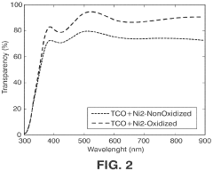
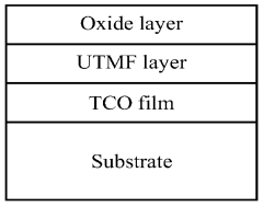
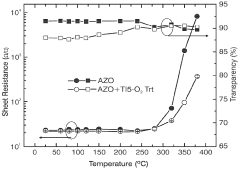
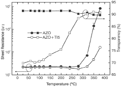
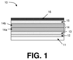
Transparent electrode based on combination of transparent conductive oxides, metals and oxides
PatentWO2011101338A2
Innovation
- A combination of transparent conductive oxides (TCOs) with an ultra-thin metal film (UTMF) and an oxide layer is proposed, where the UTMF is oxidized or covered by an oxide layer to enhance stability, compatibility, and reduce transparency loss, using materials like indium tin oxide, doped zinc oxide, and metals like Cu, Ni, and Cr, with a conductive mesh or nanowires for improved performance.
Method for fabricating organic optoelectronic devices and organic devices thereby obtained
PatentInactiveEP2256839A2
Innovation
- The use of doped metal oxide layers with enhanced electrical conductivity, formed through methods like thermal evaporation or electron beam evaporation, allows for thicker layers without increasing series resistance or reducing transparency, providing a buffer or optical spacer function while minimizing damage to underlying organic layers.


Manufacturing Scalability of TCO-Based Photonic Devices
The manufacturing scalability of TCO-based photonic devices represents a critical factor in their commercial viability and widespread adoption. Current manufacturing processes for TCO integration in photonic devices face several challenges that must be addressed to achieve industrial-scale production. The deposition techniques for TCOs, including sputtering, chemical vapor deposition, and sol-gel methods, each present different scalability profiles and quality-consistency trade-offs.
Sputtering processes, while offering excellent film uniformity, face challenges in scaling to larger substrate sizes without compromising material properties. The industry has made significant progress in developing large-area sputtering systems, but maintaining precise stoichiometry and crystallinity across larger areas remains problematic. Chemical vapor deposition methods offer better conformality but struggle with precursor utilization efficiency at scale, increasing production costs.
Temperature sensitivity during TCO deposition presents another manufacturing challenge. Many high-performance TCOs require elevated processing temperatures that can damage underlying device structures or create thermal stress. Recent developments in low-temperature processing techniques, including room-temperature sputtering with post-deposition treatments, show promise for overcoming this limitation.
Integration of TCO deposition into existing semiconductor fabrication lines represents a significant hurdle. The compatibility of TCO processing with standard CMOS fabrication requires careful engineering of process flows and contamination control. Several foundries have begun implementing dedicated process modules for TCO integration, though standardization remains limited.
Patterning of TCO layers at nanoscale dimensions necessary for advanced photonic devices presents additional manufacturing challenges. Traditional photolithography and etching processes must be optimized specifically for TCO materials to achieve the required feature resolution while maintaining optical and electrical properties. Emerging techniques such as nanoimprint lithography offer potential solutions but require further development for high-volume manufacturing.
Cost considerations significantly impact manufacturing scalability. While raw material costs for common TCOs like ITO remain relatively stable, the specialized deposition equipment and process complexity add substantial manufacturing overhead. Alternative TCO materials such as aluminum-doped zinc oxide (AZO) offer cost advantages but may require process modifications to achieve comparable performance.
Yield management represents perhaps the most critical aspect of manufacturing scalability. Defect densities in TCO films directly impact device performance, and detection methods must be refined to identify optical and electrical defects early in the production process. Several equipment manufacturers have developed in-line monitoring tools specifically for TCO quality control, enabling real-time process adjustments.
Sustainability Aspects of TCO Materials Production
The sustainability of Transparent Conductive Oxide (TCO) materials production represents a critical consideration in the broader adoption of photonic integrated devices. Traditional TCO manufacturing processes, particularly for industry standards like Indium Tin Oxide (ITO), involve energy-intensive sputtering techniques and rare earth elements that raise significant environmental concerns. The extraction of indium, a key component in ITO, has been associated with substantial ecological disruption and resource depletion, with current global reserves facing increasing pressure from growing demand across multiple technology sectors.
Life cycle assessments of TCO production reveal considerable carbon footprints, primarily stemming from high-temperature deposition processes and the energy requirements for material purification. For instance, the production of one square meter of ITO-coated glass can generate approximately 2-3 kg CO2 equivalent emissions, highlighting the environmental impact of these essential photonic materials.
Water consumption presents another sustainability challenge, with wet etching processes and cleaning steps in TCO fabrication requiring significant volumes of ultra-pure water and potentially generating contaminated wastewater containing heavy metals and acid residues. Advanced treatment systems are increasingly being implemented to mitigate these impacts, though they add complexity and cost to production facilities.
Recent innovations are addressing these sustainability concerns through several promising approaches. Alternative TCO materials such as aluminum-doped zinc oxide (AZO) and fluorine-doped tin oxide (FTO) utilize more abundant elements, reducing dependence on scarce resources. Additionally, low-temperature deposition techniques including solution-based processing and atmospheric pressure chemical vapor deposition are emerging as energy-efficient alternatives to conventional vacuum-based methods.
Circular economy principles are gradually being applied to TCO production, with research focusing on recovery and recycling methodologies for indium and other valuable materials from end-of-life devices. Some manufacturers have implemented closed-loop systems that recapture and reuse process chemicals, significantly reducing waste generation and resource consumption.
Regulatory frameworks worldwide are increasingly emphasizing sustainable materials production, with initiatives like the European Union's Restriction of Hazardous Substances (RoHS) Directive and Extended Producer Responsibility (EPR) schemes driving industry transformation. These regulations, coupled with growing consumer awareness, are incentivizing manufacturers to develop greener TCO production methods and transparent supply chains that demonstrate environmental responsibility throughout the material lifecycle.
Unlock deeper insights with Patsnap Eureka Quick Research — get a full tech report to explore trends and direct your research. Try now!
Generate Your Research Report Instantly with AI Agent
Supercharge your innovation with Patsnap Eureka AI Agent Platform!