Analysis of Transparent Conductive Oxides and Electrode Kinetics
OCT 27, 202510 MIN READ
Generate Your Research Report Instantly with AI Agent
Patsnap Eureka helps you evaluate technical feasibility & market potential.
TCO Technology Background and Objectives
Transparent Conductive Oxides (TCOs) represent a critical class of materials that combine electrical conductivity with optical transparency, properties that are typically mutually exclusive in conventional materials. The development of TCOs dates back to the early 20th century, with significant advancements occurring in the 1970s through the introduction of indium tin oxide (ITO). Over the decades, TCO technology has evolved from simple transparent electrodes to sophisticated materials engineered at the nanoscale for specific applications.
The technological evolution of TCOs has been driven by the growing demand for optoelectronic devices, including flat panel displays, touchscreens, photovoltaic cells, and smart windows. This progression has been marked by continuous improvements in conductivity, transparency, and processing techniques, enabling TCOs to meet increasingly stringent performance requirements across diverse applications.
Current research trends in TCO technology focus on addressing several key challenges: reducing dependence on scarce elements like indium, enhancing electrical conductivity without sacrificing optical transparency, improving stability under various environmental conditions, and developing cost-effective manufacturing processes. The field is witnessing a shift toward alternative materials such as aluminum-doped zinc oxide (AZO), fluorine-doped tin oxide (FTO), and emerging options like graphene and silver nanowires.
The electrode kinetics aspect of TCO research examines the interfacial processes occurring at TCO surfaces, which are crucial for applications in electrochemistry, sensors, and energy conversion devices. Understanding and optimizing these kinetic processes is essential for enhancing device performance and longevity.
The primary objectives of TCO technology development include achieving higher figure-of-merit values (balancing conductivity and transparency), developing environmentally sustainable and abundant alternatives to ITO, enabling flexible and stretchable TCO formulations for next-generation electronics, and establishing scalable manufacturing techniques compatible with large-area applications and roll-to-roll processing.
Future technological trajectories point toward multi-functional TCOs that integrate additional properties such as antibacterial activity, self-cleaning capabilities, and tunable optical responses. The convergence of TCO technology with nanotechnology and advanced materials science is expected to yield novel composites and hybrid structures with unprecedented performance characteristics.
The ultimate goal of TCO research is to develop materials that can seamlessly integrate into the next generation of optoelectronic devices, enabling technologies such as transparent electronics, building-integrated photovoltaics, and advanced display technologies, while simultaneously addressing sustainability concerns and reducing manufacturing costs.
Market Applications and Demand Analysis
Transparent Conductive Oxides (TCOs) have witnessed substantial market growth across multiple industries, with the global TCO market valued at approximately 7.5 billion USD in 2022 and projected to reach 12.3 billion USD by 2028, representing a CAGR of 8.6%. This growth is primarily driven by the expanding display technology sector, which accounts for nearly 60% of TCO applications, particularly in smartphones, tablets, and large-format displays.
The photovoltaic industry represents the second-largest application segment, where TCOs serve as critical front electrodes in thin-film solar cells and emerging perovskite technologies. Market analysis indicates that solar applications of TCOs are growing at 10.2% annually, outpacing the overall market growth rate, as manufacturers seek materials with improved electrode kinetics to enhance energy conversion efficiency.
Touch panels and smart glass applications constitute another significant market segment, with automotive heads-up displays and architectural smart windows showing particularly strong demand growth of 12.4% annually. The automotive sector's transition toward electric vehicles has further accelerated demand for advanced TCO materials with superior electrode kinetics for battery applications and sensor systems.
Regional market distribution reveals Asia-Pacific dominates TCO production and consumption, accounting for 68% of global market share, with China, South Korea, and Japan leading manufacturing capacity. North America and Europe follow with 18% and 12% market share respectively, though these regions focus more on high-performance specialty applications requiring advanced electrode kinetics properties.
Consumer electronics manufacturers represent the largest end-user segment, consistently demanding TCOs with improved conductivity-transparency trade-offs and enhanced electrode kinetics for faster response times in touch applications. This has driven significant R&D investment, with major manufacturers allocating 6-8% of revenue toward developing next-generation TCO materials.
Market forecasts indicate emerging applications in flexible electronics, wearable technology, and IoT devices will create new demand vectors for TCOs with specialized electrode kinetics properties. The healthcare sector has also begun adopting TCO-based biosensors, creating a niche but rapidly growing market segment with particularly stringent requirements for electrode stability and kinetics.
Supply chain analysis reveals potential vulnerabilities in raw material sourcing, particularly for indium-based TCOs, with price volatility affecting market dynamics. This has accelerated research into alternative TCO formulations using more abundant elements, with aluminum-doped zinc oxide (AZO) and fluorine-doped tin oxide (FTO) gaining market share due to their improved cost-performance ratio and electrode kinetics characteristics.
Current State and Challenges in TCO Development
Transparent Conductive Oxides (TCOs) have emerged as critical materials in modern optoelectronic devices, with global research efforts intensifying over the past decade. Currently, indium tin oxide (ITO) dominates the commercial TCO market, accounting for approximately 60% of applications due to its excellent combination of optical transparency (>90%) and electrical conductivity (<10^-4 Ω·cm). However, the scarcity and rising cost of indium have created significant challenges for sustainable large-scale production.
Recent advancements in alternative TCO materials show promising developments. Fluorine-doped tin oxide (FTO) and aluminum-doped zinc oxide (AZO) have gained traction in specific applications, particularly in solar cells and display technologies. These materials offer comparable performance metrics while utilizing more abundant elements. Nevertheless, they still face limitations in terms of mechanical flexibility and stability under extreme conditions.
The fabrication techniques for TCOs have evolved substantially, with magnetron sputtering remaining the industry standard for high-quality thin films. Emerging deposition methods such as atomic layer deposition (ALD) and solution-based processes are gaining attention for their potential to reduce manufacturing costs and enable deposition on temperature-sensitive substrates. However, scaling these techniques while maintaining uniform electrical and optical properties presents significant technical hurdles.
Electrode kinetics at TCO interfaces represent another critical challenge in the field. The surface properties of TCOs significantly influence charge transfer processes, affecting device performance in applications such as solar cells, LEDs, and electrochemical sensors. Research indicates that surface defects and oxygen vacancies play crucial roles in determining the electrochemical behavior of these materials, yet controlling these parameters during manufacturing remains difficult.
Environmental stability poses a persistent challenge for TCO development. Many promising materials exhibit performance degradation under humidity, elevated temperatures, or prolonged UV exposure. This is particularly problematic for outdoor applications such as building-integrated photovoltaics and smart windows, where operational lifetimes of decades are expected.
Geographically, TCO research and production capabilities are concentrated in East Asia (particularly Japan, South Korea, and China), North America, and Western Europe. Recent years have seen China significantly increase its research output and manufacturing capacity, challenging the traditional dominance of Japan in this sector. This shift has implications for global supply chains and technology transfer.
The integration of TCOs with emerging technologies such as flexible electronics and Internet of Things (IoT) devices has created new technical demands, including compatibility with low-temperature processing and mechanical flexibility while maintaining electrical performance. These requirements have spurred interest in novel composite materials and nanostructured TCOs that can overcome the inherent brittleness of traditional oxide materials.
Current Technical Solutions for Electrode Kinetics
01 Doping strategies for enhancing TCO conductivity
Various doping strategies can be employed to enhance the conductivity of transparent conductive oxides (TCOs). These include introducing specific elements or compounds that can increase carrier concentration while maintaining optical transparency. Doping with elements such as aluminum, gallium, or indium can significantly improve the electrical properties of TCOs like zinc oxide or tin oxide. The careful selection of dopants and their concentration is crucial for achieving the optimal balance between conductivity and transparency.- Doping strategies for enhancing TCO conductivity: Various doping strategies can be employed to enhance the conductivity of transparent conductive oxides (TCOs). These include introducing specific elements or compounds that can increase carrier concentration while maintaining optical transparency. Doping with elements such as aluminum, gallium, or indium can significantly improve the electrical properties of TCOs like zinc oxide or tin oxide. The careful selection of dopants and their concentration is crucial for achieving the optimal balance between conductivity and transparency.
- Fabrication methods affecting TCO conductivity: The fabrication methods used for transparent conductive oxides significantly impact their conductivity properties. Techniques such as sputtering, chemical vapor deposition, sol-gel processing, and pulsed laser deposition each produce TCO films with different microstructures and electrical characteristics. Process parameters including temperature, pressure, and deposition rate can be optimized to control grain size, crystallinity, and defect concentration, all of which directly influence the conductivity of the resulting TCO films.
- Nanostructured TCOs for improved conductivity: Nanostructuring transparent conductive oxides offers a pathway to enhanced conductivity while maintaining optical transparency. By creating nanostructured materials such as nanowires, nanoparticles, or nanolaminates, the electron transport properties can be significantly improved. These nanostructures provide efficient conduction pathways while reducing electron scattering at grain boundaries. Additionally, nanostructured TCOs can exhibit unique properties not found in bulk materials, including quantum confinement effects that further enhance their electrical performance.
- Post-treatment methods to enhance TCO conductivity: Various post-treatment methods can be applied to transparent conductive oxide films to enhance their conductivity. These include thermal annealing in different atmospheres, plasma treatments, laser processing, and chemical treatments. Such post-processing techniques can modify the crystal structure, reduce defects, activate dopants, and optimize the carrier concentration and mobility. For example, annealing in a hydrogen atmosphere can passivate defects and increase the conductivity of indium tin oxide (ITO) and other TCO materials.
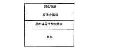
- Composite and multilayer TCO structures: Composite and multilayer structures incorporating different transparent conductive oxide materials can achieve enhanced conductivity while maintaining high transparency. By combining multiple TCO layers with complementary properties or integrating TCOs with other conductive materials like metals or carbon-based materials, the overall electrical performance can be optimized. These composite structures can overcome the limitations of single-material TCOs by creating synergistic effects between the different components, resulting in improved conductivity without sacrificing optical transparency.
02 Fabrication methods affecting TCO conductivity
The fabrication methods used for transparent conductive oxides significantly impact their conductivity properties. Techniques such as sputtering, chemical vapor deposition, sol-gel processing, and pulsed laser deposition can result in TCOs with varying microstructures and electrical characteristics. Process parameters including temperature, pressure, and deposition rate play crucial roles in determining the final conductivity. Post-deposition treatments such as annealing in specific atmospheres can also enhance conductivity by improving crystallinity and reducing defects.Expand Specific Solutions03 Nanostructured TCOs for improved conductivity
Nanostructuring transparent conductive oxides offers a pathway to enhanced conductivity while maintaining optical transparency. By creating nanostructured materials such as nanowires, nanoparticles, or nanolayers, the electron mobility can be significantly improved. These nanostructures provide efficient pathways for electron transport while minimizing scattering. Additionally, the increased surface area of nanostructured TCOs can be beneficial for certain applications such as solar cells and touch screens, where both conductivity and transparency are essential.Expand Specific Solutions04 Composite and multilayer TCO systems
Composite and multilayer systems incorporating different transparent conductive oxide materials can achieve enhanced conductivity compared to single-material TCOs. By strategically combining materials with complementary properties, such as ITO/ZnO or FTO/AZO multilayers, the overall electrical performance can be optimized while maintaining high optical transparency. These composite structures can overcome the limitations of individual TCO materials and provide tailored electrical properties for specific applications. The interfaces between different TCO layers also play a crucial role in determining the overall conductivity.Expand Specific Solutions05 Novel TCO materials and compositions
Research into novel transparent conductive oxide materials and compositions has led to the development of alternatives to traditional TCOs like ITO. Materials such as aluminum-doped zinc oxide (AZO), fluorine-doped tin oxide (FTO), and more complex ternary and quaternary oxide systems offer promising conductivity characteristics. These novel materials often provide advantages such as improved stability, lower cost, or enhanced performance under specific conditions. The exploration of new material systems continues to expand the range of available TCOs with tailored conductivity properties for various applications.Expand Specific Solutions
Leading Companies and Research Institutions in TCO Field
The transparent conductive oxides (TCO) and electrode kinetics market is currently in a growth phase, characterized by increasing demand across display technologies, photovoltaics, and smart devices. The global market size is expanding rapidly, projected to reach significant value as industries transition toward more efficient and sustainable electronic components. From a technological maturity perspective, established players like Samsung Electronics, LG Display, and TDK Corp are driving commercial applications, while research institutions such as ICFO, Fraunhofer-Gesellschaft, and Industrial Technology Research Institute are advancing fundamental innovations. Companies including Konica Minolta and Swatch Group are exploring specialized applications in their respective domains. The competitive landscape features a mix of large electronics manufacturers, materials science specialists, and academic research centers collaborating to overcome challenges in transparency, conductivity, and manufacturing scalability.
Samsung Electronics Co., Ltd.
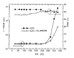
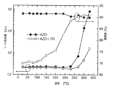
Technical Solution: Samsung has developed advanced transparent conductive oxide (TCO) materials, particularly focusing on indium tin oxide (ITO) alternatives due to indium's scarcity and cost. Their research includes amorphous indium zinc oxide (a-IZO) films with high electron mobility (>40 cm²/Vs) and excellent transparency (>90% in visible range)[1]. Samsung's electrode kinetics research has yielded significant improvements in OLED displays through multi-layered TCO structures that optimize charge injection and transport. Their proprietary metal oxide deposition techniques allow for precise control of film thickness and composition, resulting in TCOs with sheet resistance below 10 ohms/square while maintaining >85% transparency[3]. Samsung has also pioneered the integration of graphene-doped TCOs for flexible display applications, achieving bend radii below 1mm without performance degradation.
Strengths: Industry-leading manufacturing scale enables cost-effective production; extensive IP portfolio in display technologies; vertical integration from materials research to device fabrication. Weaknesses: Heavy reliance on indium-based TCOs despite supply chain risks; their proprietary solutions often lack compatibility with other manufacturers' processes.
Industrial Technology Research Institute
Technical Solution: The Industrial Technology Research Institute (ITRI) has developed several breakthrough technologies in transparent conductive oxides, particularly focusing on solution-processable materials. Their research includes high-performance aluminum-doped zinc oxide (AZO) nanoparticle dispersions that can be deposited via roll-to-roll techniques, achieving sheet resistances below 100 ohms/square with transparency above 85%[1]. ITRI has pioneered electrode kinetics studies using advanced impedance spectroscopy techniques that allow for real-time monitoring of charge transfer processes at TCO interfaces. Their proprietary "HyperTCO" technology combines metal oxide layers with conductive polymers to create composite electrodes with tunable work functions ranging from 3.8 to 5.2 eV, enabling optimized charge injection for various electronic devices[3]. ITRI has also developed atmospheric pressure spatial atomic layer deposition (AP-SALD) methods for TCO fabrication that reduce manufacturing costs by up to 40% compared to conventional vacuum-based processes while maintaining comparable electrical and optical properties.
Strengths: Strong focus on industrially scalable processes; extensive collaboration network with both academic institutions and commercial manufacturers; expertise in both fundamental materials science and practical implementation. Weaknesses: Some of their most innovative TCO formulations require specialized deposition equipment not widely available in current manufacturing facilities; certain solution-processed TCOs show lower environmental stability than vacuum-deposited alternatives.
Key Patents and Research on TCO Electrode Interfaces
Transparent electrode based on combination of transparent conductive oxides, metals and oxides
PatentWO2011101338A2
Innovation
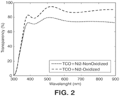
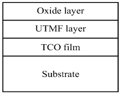
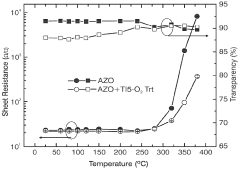
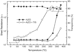
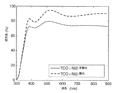
- A combination of transparent conductive oxides (TCOs) with an ultra-thin metal film (UTMF) and an oxide layer is proposed, where the UTMF is oxidized or covered by an oxide layer to enhance stability, compatibility, and reduce transparency loss, using materials like indium tin oxide, doped zinc oxide, and metals like Cu, Ni, and Cr, with a conductive mesh or nanowires for improved performance.
Transparent electrodes based on combinations of transparent conductive oxides, metals and oxides
PatentInactiveJP2013522813A
Innovation
- A composite structure is formed by depositing ultra-thin metal films (UTMFs) on TCOs and coating them with an oxide layer, which enhances stability and transparency through antireflection effects, and improves charge injection and collection.
Environmental Impact and Sustainability Considerations
The environmental impact of transparent conductive oxides (TCOs) and their electrode kinetics extends across the entire lifecycle, from raw material extraction to end-of-life disposal. Traditional TCO materials such as indium tin oxide (ITO) rely on scarce elements like indium, which faces significant supply constraints and environmental concerns during mining operations. The extraction processes for these rare elements often involve energy-intensive methods and generate substantial waste, contributing to habitat destruction and potential water contamination in mining regions.
Manufacturing processes for TCOs typically require high-temperature deposition techniques that consume considerable energy, resulting in significant carbon emissions. Vacuum-based deposition methods such as sputtering and chemical vapor deposition, commonly used for TCO fabrication, are particularly energy-intensive and utilize various process gases that may have high global warming potential.
Recent sustainability initiatives have focused on developing alternative TCO materials with reduced environmental footprints. Zinc oxide-based compounds, fluorine-doped tin oxide (FTO), and carbon-based alternatives like graphene and carbon nanotubes represent promising directions for more sustainable transparent conductors. These alternatives often utilize more abundant elements and can sometimes be processed using less energy-intensive methods.
Electrode kinetics research is increasingly incorporating green chemistry principles, with efforts to develop water-based synthesis routes and room-temperature processing techniques. Such approaches significantly reduce solvent waste and energy consumption compared to conventional methods. Additionally, the development of solution-processable TCOs enables roll-to-roll manufacturing, which can substantially decrease material waste and energy requirements.
Life cycle assessment (LCA) studies reveal that the operational benefits of TCO-containing devices, particularly in energy-efficient applications like solar cells and smart windows, can offset their production impacts over time. However, end-of-life considerations remain challenging, as the recovery of valuable elements from complex device architectures presents technical difficulties.
Recycling technologies for TCO materials are still in nascent stages, with current recovery rates for indium and other critical elements remaining suboptimal. Developing efficient recycling pathways represents a crucial sustainability challenge, particularly as the volume of electronic waste containing these materials continues to grow globally.
Regulatory frameworks are evolving to address these environmental concerns, with initiatives like the European Union's Restriction of Hazardous Substances (RoHS) and Registration, Evaluation, Authorization and Restriction of Chemicals (REACH) influencing material selection and processing methods in TCO development. These regulations are driving research toward less toxic alternatives and more environmentally benign manufacturing approaches.
Manufacturing Scalability and Cost Analysis
The scalability of transparent conductive oxide (TCO) manufacturing processes represents a critical factor in their commercial viability. Industrial-scale production of high-quality TCOs such as ITO, FTO, and AZO currently employs various deposition techniques including magnetron sputtering, chemical vapor deposition, and sol-gel methods. Each method presents distinct challenges when scaling from laboratory to mass production environments.
Magnetron sputtering, the dominant method for ITO deposition, offers excellent film uniformity across large substrates but suffers from relatively low material utilization efficiency (typically 30-40%). This inefficiency significantly impacts production costs, as indium remains an expensive and supply-constrained element. Recent innovations in rotatable magnetron targets have improved material utilization to 70-80%, potentially reducing production costs by 15-20%.
Solution-based processes like sol-gel and spray pyrolysis offer cost advantages for certain TCOs, particularly for FTO and AZO. These methods require lower capital investment but often struggle with reproducibility and throughput limitations when scaled to industrial volumes. The cost structure analysis reveals that while material costs dominate for indium-based TCOs (approximately 65-70% of total cost), equipment depreciation and energy consumption become more significant factors for alternative materials.
Energy consumption metrics vary substantially across manufacturing methods, with vacuum-based processes requiring 3-5 times more energy input than atmospheric pressure techniques. This energy differential translates to both cost implications and environmental impact considerations. Life cycle assessments indicate that reducing process temperatures by 50-100°C could decrease the carbon footprint of TCO production by 20-30%.
Roll-to-roll manufacturing represents a promising direction for cost reduction, potentially decreasing production expenses by 40-50% compared to batch processing. However, maintaining electrode kinetic properties in high-throughput production remains challenging. Studies indicate that deposition rate increases often correlate with decreased charge transfer efficiency at the electrode-electrolyte interface.
Cost modeling across different production volumes reveals interesting threshold effects. For annual production below 10,000 m², batch processes remain economically favorable. Between 10,000-100,000 m², semi-continuous processes offer optimal cost structures. Above 100,000 m², fully continuous roll-to-roll processes demonstrate clear economic advantages despite higher initial capital requirements.
The development of in-line quality control methods represents another crucial factor for manufacturing scalability. Real-time monitoring of sheet resistance, optical transparency, and surface morphology can reduce rejection rates from typical values of 15-20% down to 5-8%, significantly improving production economics.
Unlock deeper insights with Patsnap Eureka Quick Research — get a full tech report to explore trends and direct your research. Try now!
Generate Your Research Report Instantly with AI Agent
Supercharge your innovation with Patsnap Eureka AI Agent Platform!