Transparent Conductive Oxides for Enhanced Electrical Performance
OCT 27, 20259 MIN READ
Generate Your Research Report Instantly with AI Agent
Patsnap Eureka helps you evaluate technical feasibility & market potential.
TCO Technology Background and Objectives
Transparent Conductive Oxides (TCOs) represent a critical class of materials that combine the seemingly contradictory properties of optical transparency and electrical conductivity. The development of TCOs dates back to the early 20th century, with the first significant breakthrough occurring in 1907 when cadmium oxide was identified as both transparent and conductive. However, the field gained substantial momentum in the 1970s with the development of indium tin oxide (ITO), which remains the industry standard despite ongoing challenges.
The evolution of TCO technology has been driven by the exponential growth of optoelectronic devices, including flat-panel displays, touchscreens, photovoltaic cells, and smart windows. This growth trajectory has been particularly steep since the early 2000s, coinciding with the proliferation of smartphones and other portable electronic devices that require transparent electrodes. The global TCO market has expanded at a compound annual growth rate exceeding 10% over the past decade, highlighting the increasing technological and commercial significance of these materials.
Current technological trends in TCO development focus on addressing several key limitations. These include reducing dependency on scarce elements like indium, enhancing electrical conductivity without sacrificing optical transparency, improving mechanical flexibility for next-generation flexible electronics, and developing cost-effective, environmentally friendly manufacturing processes. Recent advances in nanotechnology and materials science have opened new avenues for TCO innovation, including nanostructured oxides, composite materials, and novel deposition techniques.
The primary technical objectives for enhanced electrical performance in TCOs center around achieving sheet resistance below 10 ohms/square while maintaining optical transparency above 90% in the visible spectrum. Additional goals include improving stability under various environmental conditions, enhancing compatibility with flexible substrates, and reducing manufacturing costs by at least 30% compared to conventional ITO-based solutions. These objectives align with the broader industry push toward more sustainable, efficient, and versatile electronic components.
Looking forward, TCO technology is expected to play a pivotal role in emerging technologies such as transparent electronics, building-integrated photovoltaics, and next-generation display technologies. The convergence of TCO research with other advanced materials, including 2D materials like graphene and transition metal dichalcogenides, presents promising opportunities for hybrid systems with unprecedented performance characteristics. The ultimate goal remains the development of TCO materials that offer optimal balance between transparency, conductivity, cost, and environmental sustainability to enable the next generation of optoelectronic devices.
Market Analysis for Transparent Conductive Materials
The transparent conductive materials market is experiencing robust growth, driven primarily by the expanding electronics industry and increasing demand for touchscreen devices. The global market value for transparent conductive materials reached approximately $5.1 billion in 2022 and is projected to grow at a compound annual growth rate (CAGR) of 8.7% through 2028, potentially reaching $8.4 billion by the end of the forecast period.
Indium Tin Oxide (ITO) continues to dominate the market, accounting for over 70% of the total market share due to its excellent combination of optical transparency and electrical conductivity. However, supply constraints and price volatility of indium are creating significant market opportunities for alternative materials such as silver nanowires, carbon nanotubes, graphene, and metal mesh technologies.
The consumer electronics segment represents the largest application area, with smartphones, tablets, and laptops driving consistent demand. The automotive industry is emerging as a rapidly growing sector, with transparent conductive materials being increasingly incorporated into advanced driver-assistance systems (ADAS), heads-up displays, and smart windows. Additionally, the photovoltaic industry is showing promising growth potential as transparent conductive oxides are essential components in thin-film solar cells.
Regionally, Asia-Pacific dominates the market with approximately 65% share, attributed to the concentration of electronics manufacturing in countries like China, South Korea, Japan, and Taiwan. North America and Europe follow, with growing applications in automotive and emerging technologies sectors respectively.
Key market challenges include the need for materials with improved flexibility for foldable and wearable devices, enhanced durability for automotive applications, and reduced production costs. The industry is witnessing a shift toward solution-processable materials that can enable roll-to-roll manufacturing, potentially reducing production costs by up to 40% compared to traditional vacuum deposition methods.
Customer requirements are evolving toward materials with sheet resistance below 50 ohms/square while maintaining optical transparency above 90% in the visible spectrum. Additionally, there is increasing demand for materials that can withstand over 100,000 bending cycles for flexible electronics applications, presenting both challenges and opportunities for material innovation.
The market is also being shaped by sustainability concerns, with growing interest in materials that reduce environmental impact and comply with regulations such as the European Union's Restriction of Hazardous Substances (RoHS) directive, particularly regarding the replacement of indium-based materials.
Current Status and Challenges in TCO Development
Transparent Conductive Oxides (TCOs) have emerged as critical materials in modern optoelectronic devices, with significant research efforts focused on enhancing their electrical performance while maintaining optical transparency. Currently, the most widely deployed TCO is Indium Tin Oxide (ITO), which dominates approximately 90% of the global market due to its excellent combination of high transparency (>85%) in the visible spectrum and low electrical resistivity (10^-4 Ω·cm).
Despite ITO's commercial success, several challenges impede its broader application. The scarcity of indium has led to price volatility and supply chain concerns, with indium being classified as a critical raw material by many countries. This has accelerated research into alternative TCO materials such as Fluorine-doped Tin Oxide (FTO), Aluminum-doped Zinc Oxide (AZO), and more recently, amorphous oxide semiconductors like IGZO (Indium Gallium Zinc Oxide).
Technical limitations also persist across TCO technologies. The fundamental trade-off between optical transparency and electrical conductivity remains a significant challenge, as mechanisms that enhance conductivity often reduce transparency. Most commercial TCOs still struggle to achieve sheet resistances below 10 Ω/sq while maintaining >90% transparency, which is increasingly required for next-generation devices.
Manufacturing scalability presents another obstacle. While vacuum-based deposition techniques like sputtering produce high-quality TCO films, they involve high capital costs and energy consumption. Solution-based processes offer cost advantages but typically yield films with inferior electrical properties and uniformity issues at industrial scales. The development gap between laboratory demonstrations and commercial-scale production remains substantial.
Stability under operational conditions represents a critical challenge for TCO implementation. Many promising materials exhibit performance degradation when exposed to humidity, elevated temperatures, or mechanical stress. AZO, for instance, shows excellent initial performance but degrades significantly in humid environments, limiting its application in unencapsulated devices.
Geographically, TCO research and production capabilities are unevenly distributed. Japan, South Korea, and Taiwan lead in high-performance TCO development and manufacturing, while China dominates in production volume. European and North American institutions contribute significantly to fundamental research but lag in commercial-scale manufacturing capabilities.
Emerging applications in flexible electronics, photovoltaics, and smart windows are driving new performance requirements that current TCOs struggle to meet. The demand for TCOs compatible with flexible substrates, low-temperature processing, and specialized properties like IR reflection or UV blocking has created specialized niches where conventional TCOs underperform, opening opportunities for novel materials and compositional engineering approaches.
Current TCO Material Solutions and Implementation
01 Composition and structure of transparent conductive oxides
Transparent conductive oxides (TCOs) can be formulated with specific compositions and structures to enhance their electrical performance. These materials typically consist of metal oxides doped with various elements to increase conductivity while maintaining optical transparency. The crystalline structure, grain boundaries, and film thickness significantly impact the electrical properties of TCOs. Optimization of these parameters can lead to improved carrier concentration and mobility, resulting in better electrical performance.- Composition and structure of transparent conductive oxides: Transparent conductive oxides (TCOs) can be formulated with specific compositions and structures to enhance their electrical performance. These materials typically include indium tin oxide (ITO), zinc oxide (ZnO), and other metal oxides that provide both optical transparency and electrical conductivity. The electrical performance can be improved by controlling the crystalline structure, grain boundaries, and stoichiometry of the oxide layers. Dopants can be incorporated to modify the carrier concentration and mobility, thereby enhancing the conductivity while maintaining transparency.
- Deposition techniques for enhanced electrical properties: Various deposition techniques can significantly impact the electrical performance of transparent conductive oxides. Methods such as sputtering, chemical vapor deposition, sol-gel processing, and atomic layer deposition can be optimized to control film thickness, uniformity, and microstructure. Process parameters including temperature, pressure, and gas composition during deposition affect the resulting electrical properties. Post-deposition treatments such as annealing can further improve crystallinity and reduce defects, leading to enhanced conductivity while maintaining optical transparency.
- Doping strategies to improve conductivity: Doping is a critical strategy for enhancing the electrical performance of transparent conductive oxides. By introducing specific elements into the oxide matrix, carrier concentration can be increased without significantly compromising transparency. Common dopants include aluminum, gallium, and fluorine for zinc oxide, tin for indium oxide, and antimony for tin oxide. The type and concentration of dopants can be optimized to achieve the desired balance between conductivity and transparency. Co-doping with multiple elements can create synergistic effects that further enhance electrical properties.
- Nanostructured TCOs for improved performance: Nanostructuring transparent conductive oxides can significantly enhance their electrical performance. Nanowires, nanoparticles, and nanolaminates offer increased surface area and unique electronic properties compared to bulk materials. These nanostructures can provide enhanced carrier mobility and reduced scattering at grain boundaries. Hierarchical structures combining different scales of features can create optimized pathways for electrical conduction. Additionally, nanocomposites incorporating carbon nanotubes or graphene with TCOs can create hybrid materials with superior electrical properties while maintaining optical transparency.
- Interface engineering for device integration: Interface engineering is crucial for optimizing the electrical performance of transparent conductive oxides in devices. The contact between TCOs and adjacent layers in electronic devices can create barriers to charge transport if not properly designed. Surface treatments, buffer layers, and work function modification can improve charge injection and extraction at interfaces. Controlling the band alignment between TCOs and semiconductors or electrodes enhances device efficiency. Additionally, passivation techniques can reduce surface defects and prevent degradation of electrical properties over time, ensuring stable performance in applications such as displays, solar cells, and touch screens.
02 Doping strategies for enhanced conductivity
Doping is a critical strategy for improving the electrical performance of transparent conductive oxides. Various dopants, such as aluminum, gallium, indium, and fluorine, can be incorporated into the oxide matrix to increase carrier concentration. The type and concentration of dopants significantly affect the electrical conductivity and optical properties of TCOs. Controlled doping processes can optimize the balance between transparency and conductivity, leading to TCOs with superior electrical performance for various applications.Expand Specific Solutions03 Deposition techniques and processing conditions
The method of deposition and processing conditions significantly impact the electrical performance of transparent conductive oxides. Techniques such as sputtering, chemical vapor deposition, sol-gel, and pulsed laser deposition can be used to create TCO films with varying properties. Post-deposition treatments, including annealing temperature, atmosphere, and duration, play crucial roles in determining the final electrical characteristics. Optimizing these parameters can enhance crystallinity, reduce defects, and improve carrier mobility, resulting in TCOs with superior electrical performance.Expand Specific Solutions04 Novel TCO materials and composites
Research into novel TCO materials and composites has led to advancements in electrical performance. Beyond traditional indium tin oxide (ITO), materials such as zinc oxide, tin oxide, and various ternary compounds offer alternative solutions with unique electrical properties. Composite structures, including multilayer films and nanocomposites, can provide enhanced electrical performance through synergistic effects. These novel materials and composites expand the range of available TCOs with tailored electrical characteristics for specific applications.Expand Specific Solutions05 Surface modification and interface engineering
Surface modification and interface engineering techniques can significantly improve the electrical performance of transparent conductive oxides. Treatments such as plasma processing, chemical etching, and surface functionalization can modify the surface properties of TCOs to enhance carrier transport. Interface engineering between TCOs and adjacent layers in devices is crucial for reducing contact resistance and improving overall electrical performance. These approaches can optimize charge transfer across interfaces and enhance the stability of electrical properties under various operating conditions.Expand Specific Solutions
Key Industry Players in TCO Research and Production
The transparent conductive oxide (TCO) market is currently in a growth phase, driven by increasing demand for high-performance electronic displays and photovoltaic applications. The global market size is estimated to exceed $7 billion, with a projected CAGR of 6-8% through 2028. Technologically, the field shows varying maturity levels across applications, with established players like Samsung Electronics, AGC Inc., and TDK Corp. leading commercial deployment while research institutions such as ICFO, Trinity College Dublin, and Industrial Technology Research Institute drive innovation in next-generation materials. Companies including Sumitomo Chemical, Idemitsu Kosan, and Semiconductor Energy Laboratory are advancing proprietary TCO formulations with enhanced electrical conductivity and optical transparency, positioning themselves strategically as the industry transitions toward flexible electronics and energy-efficient applications.
Sumitomo Chemical Co., Ltd.
Technical Solution: Sumitomo Chemical has developed a comprehensive TCO technology platform focused on solution-processable materials for cost-effective manufacturing. Their SUMI-TCO™ product line features metal oxide nanoparticle dispersions that can be deposited via printing techniques, eliminating the need for vacuum-based deposition methods. These materials achieve sheet resistance of 50-100 Ω/sq with transparency above 80%[2]. Sumitomo has particularly advanced the field of antimony-doped tin oxide (ATO) and fluorine-doped tin oxide (FTO) materials, which offer enhanced environmental stability compared to conventional ITO. Their patented surface modification technology improves the interface between TCO layers and adjacent organic materials, reducing contact resistance in optoelectronic devices[4]. Recent developments include composite TCO structures that combine different metal oxide layers to achieve synergistic electrical and optical properties, with demonstrated improvements in device efficiency of up to 15% in organic photovoltaics[7].
Strengths: Solution-processable materials enable lower manufacturing costs; strong expertise in interface engineering for improved device performance; environmentally stable TCO formulations. Weaknesses: Generally higher sheet resistance compared to vacuum-deposited alternatives; challenges in achieving uniform electrical properties over large areas with solution processes; limited flexibility compared to emerging nanomaterial-based TCOs.
AGC, Inc. (Japan)
Technical Solution: AGC has developed advanced transparent conductive oxide (TCO) films based on indium tin oxide (ITO) with enhanced electrical performance. Their proprietary sputtering deposition technology enables precise control of film thickness and composition, resulting in TCOs with sheet resistance as low as 8 Ω/sq while maintaining over 85% optical transparency in the visible spectrum[1]. AGC has also pioneered the development of indium-free TCOs using zinc oxide doped with aluminum (AZO) and gallium (GZO), addressing indium scarcity concerns. Their EXCLEAR® flexible TCO films incorporate a unique mesh structure that maintains conductivity even under repeated bending, making them suitable for flexible display applications[3]. AGC's recent innovations include high-mobility amorphous TCOs that combine the advantages of crystalline and amorphous structures, achieving electron mobility exceeding 40 cm²/Vs while maintaining amorphous stability[5].
Strengths: Industry-leading optical transparency combined with low sheet resistance; advanced manufacturing capabilities for large-area deposition; proprietary technology for flexible TCOs. Weaknesses: Higher production costs compared to emerging alternatives; continued reliance on indium for premium products despite efforts to develop alternatives; challenges in scaling new TCO technologies to mass production.
Critical Patents and Innovations in TCO Technology
Composition of Transparent Conductive Material and Method for Fabricating the same
PatentPendingUS20240038912A1
Innovation
- A film structure comprising a transparent conductive oxide layer, a wide-bandgap semiconductor oxide layer, and an interface layer with controlled doping and composition, allowing for enhanced carrier mobility and conductivity while maintaining transparency, achieved through pulsed laser deposition and careful layer engineering.
Conductive structure and electronic device comprising same
PatentWO2016148514A1
Innovation
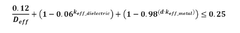
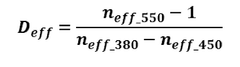
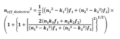
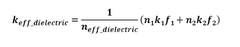
- A conductive structure comprising a first dielectric layer with a first metal compound, a second dielectric layer with a second metal compound, and a metal layer in between, optimized to satisfy specific equations that balance refractive index dispersion, extinction coefficients, and thickness ratios to achieve high light transmittance with minimal changes across the visible spectrum.
Sustainability and Environmental Impact of TCO Materials
The environmental impact of Transparent Conductive Oxide (TCO) materials has become increasingly significant as their application expands across various industries. Traditional TCO materials like Indium Tin Oxide (ITO) face sustainability challenges due to the scarcity of indium, which is classified as a critical raw material with limited global reserves. This scarcity has driven research toward alternative TCO materials with reduced environmental footprints while maintaining or enhancing electrical performance.
Life cycle assessment (LCA) studies of TCO materials reveal considerable environmental impacts during extraction and processing phases. The mining of rare elements used in TCOs contributes to habitat destruction, water pollution, and energy-intensive refining processes. For instance, indium extraction typically occurs as a byproduct of zinc mining, resulting in significant carbon emissions and resource depletion. These environmental costs must be factored into the overall sustainability evaluation of TCO technologies.
Recent advances in TCO development have focused on earth-abundant alternatives such as aluminum-doped zinc oxide (AZO), fluorine-doped tin oxide (FTO), and graphene-based composites. These materials not only address supply chain vulnerabilities but also demonstrate reduced environmental impact during production. For example, AZO manufacturing processes can achieve up to 35% lower carbon footprint compared to conventional ITO production methods, while maintaining comparable electrical conductivity and optical transparency.
The recyclability of TCO materials presents another critical sustainability dimension. End-of-life management for devices containing TCOs often faces technical challenges in material separation and recovery. Innovative recycling technologies, including hydrometallurgical processes and selective etching techniques, are being developed to recover valuable elements from discarded electronic devices. These approaches could potentially close the material loop and significantly reduce the environmental burden of TCO production.
Energy efficiency during the operational phase of TCO-containing devices also contributes to their overall environmental profile. Advanced TCO materials with enhanced electrical conductivity can reduce energy consumption in applications such as solar cells, displays, and smart windows. For instance, high-performance TCOs in photovoltaic applications can improve conversion efficiency by 2-3%, translating to substantial energy savings over the device lifetime.
Regulatory frameworks and industry standards increasingly incorporate sustainability metrics for TCO materials. The European Union's Restriction of Hazardous Substances (RoHS) directive and the Registration, Evaluation, Authorization and Restriction of Chemicals (REACH) regulation have prompted manufacturers to develop TCO formulations with reduced toxicity and environmental impact. These regulatory pressures, combined with corporate sustainability initiatives, are accelerating the transition toward greener TCO alternatives in commercial applications.
Manufacturing Scalability and Cost Analysis
The scalability of transparent conductive oxide (TCO) manufacturing processes represents a critical factor in their commercial viability and widespread adoption. Current industrial production of TCOs primarily relies on physical vapor deposition (PVD) methods, particularly magnetron sputtering, which offers excellent uniformity and throughput for large-area substrates. However, the capital equipment costs for high-quality sputtering systems remain substantial, often exceeding $1-2 million for production-scale machinery.
Material costs constitute another significant component of TCO manufacturing economics. Indium tin oxide (ITO), the industry standard, faces persistent supply chain vulnerabilities due to indium's limited availability and geopolitical supply constraints. Raw material costs for indium have fluctuated between $500-900/kg in recent years, driving research into alternative TCO compositions. Alternative materials such as aluminum-doped zinc oxide (AZO) and fluorine-doped tin oxide (FTO) offer material cost reductions of approximately 60-80% compared to ITO.
Energy consumption during TCO deposition presents both economic and environmental challenges. Traditional sputtering processes typically require vacuum environments and high power densities, resulting in energy costs of 5-8 kWh per square meter of coated surface. Solution-based deposition methods, including sol-gel and spray pyrolysis, demonstrate potential for reducing energy requirements by 30-50%, though often at the expense of electrical performance.
Yield rates and quality control metrics significantly impact overall manufacturing economics. Current industrial processes achieve yield rates of 85-95% for high-quality TCO films, with defect densities below 0.1 defects/cm². Implementing advanced in-line monitoring systems using optical and electrical characterization techniques has proven effective in maintaining quality while minimizing material waste.
The integration of TCO deposition into existing manufacturing lines represents a substantial consideration for adoption. Roll-to-roll processing shows particular promise for flexible electronics applications, potentially reducing production costs by 40-60% compared to batch processing methods. However, maintaining consistent electrical properties across large areas remains challenging, with typical variations in sheet resistance of ±10-15% across a single production run.
Cost modeling analyses indicate that at production scales exceeding 1 million square meters annually, the total manufacturing cost for high-performance TCO films ranges from $3-12 per square meter, depending on material selection and performance requirements. Emerging atmospheric pressure deposition techniques could potentially reduce these costs by an additional 20-30% while maintaining comparable electrical performance, representing a promising direction for future manufacturing innovation.
Unlock deeper insights with Patsnap Eureka Quick Research — get a full tech report to explore trends and direct your research. Try now!
Generate Your Research Report Instantly with AI Agent
Supercharge your innovation with Patsnap Eureka AI Agent Platform!