Transparent Conductive Oxides and Their Role in Printed Electronics
OCT 27, 20259 MIN READ
Generate Your Research Report Instantly with AI Agent
Patsnap Eureka helps you evaluate technical feasibility & market potential.
TCO Development History and Objectives
Transparent Conductive Oxides (TCOs) emerged in the early 20th century with the discovery of cadmium oxide's conductive properties in 1907. However, significant development began in the 1940s with the introduction of tin-doped indium oxide (ITO), which revolutionized the field due to its exceptional combination of optical transparency and electrical conductivity. The 1970s marked a pivotal era as the electronics industry expanded, creating substantial demand for transparent electrodes in display technologies.
The evolution of TCOs has been driven by the continuous need for materials that balance transparency, conductivity, and processability. Initially focused on ITO, the field has progressively diversified to address ITO's limitations, particularly its brittleness, scarcity of indium, and high processing temperatures. This diversification accelerated in the 1990s with the development of alternative TCOs such as fluorine-doped tin oxide (FTO) and aluminum-doped zinc oxide (AZO).
The 2000s witnessed a paradigm shift with the emergence of printed electronics, creating new requirements for TCO materials. This shift necessitated TCOs compatible with solution-processing techniques and low-temperature fabrication methods. The primary objective evolved from merely achieving high performance to developing materials suitable for flexible substrates and large-area manufacturing processes.
Recent technological objectives have focused on creating TCOs that maintain performance while addressing sustainability concerns. Research has intensified on earth-abundant alternatives to indium-based compounds, with particular attention to zinc-based and titanium-based oxides. Additionally, efforts have concentrated on developing TCOs compatible with ambient processing conditions to reduce energy consumption during manufacturing.
The current trajectory of TCO development aims to meet the demands of next-generation printed electronics, including flexibility, stretchability, and compatibility with additive manufacturing techniques. Researchers are exploring nanostructured TCOs, composite materials, and hybrid organic-inorganic systems to achieve unprecedented combinations of properties. The field is increasingly interdisciplinary, incorporating insights from materials science, chemistry, and electrical engineering.
Looking forward, TCO development objectives include achieving sheet resistances below 10 ohms/square with optical transmittance exceeding 90% in visible light, while using earth-abundant materials and low-energy processing methods. Additional goals include enhancing mechanical durability for flexible applications and developing TCOs with tunable work functions to optimize interfaces in complex electronic devices. These objectives align with the broader trend toward sustainable, scalable electronics manufacturing.
Market Analysis for TCO in Printed Electronics
The global market for Transparent Conductive Oxides (TCOs) in printed electronics is experiencing robust growth, driven by increasing demand for flexible displays, touch panels, photovoltaics, and smart packaging. Current market valuations place the TCO segment at approximately 4.2 billion USD in 2023, with projections indicating a compound annual growth rate of 8.7% through 2030.
Indium Tin Oxide (ITO) continues to dominate the TCO market with over 70% market share due to its established manufacturing ecosystem and superior optical-electrical performance balance. However, supply constraints and price volatility of indium are creating significant market opportunities for alternative TCOs such as Aluminum-doped Zinc Oxide (AZO), Fluorine-doped Tin Oxide (FTO), and emerging materials like graphene and silver nanowires.
Regional analysis reveals Asia-Pacific as the dominant manufacturing hub, accounting for approximately 65% of global TCO production, with China, South Korea, and Japan leading in both production capacity and technological innovation. North America and Europe follow with strengths in research and development of next-generation TCO materials and applications.
The printed electronics sector specifically represents a high-growth application area for TCOs, expanding at nearly 12% annually as industries adopt flexible, lightweight electronic solutions. Consumer electronics remains the largest end-use segment, followed by automotive displays, energy harvesting devices, and healthcare monitoring systems.
Market dynamics are increasingly influenced by sustainability concerns, with manufacturers facing pressure to develop indium-free alternatives and implement recycling programs for rare materials. This trend is accelerating research into earth-abundant TCO formulations that maintain performance while reducing environmental impact and supply chain vulnerabilities.
Price sensitivity varies significantly across application segments, with high-volume consumer electronics manufacturers prioritizing cost reduction, while emerging applications in healthcare and IoT devices emphasize performance metrics over price considerations. The average selling price for TCO materials has decreased by approximately 5% annually over the past five years due to manufacturing efficiencies and increased competition.
Industry forecasts indicate that flexible and stretchable electronics will drive the next wave of TCO market expansion, with printed solar cells and wearable technology representing particularly promising growth vectors. The integration of TCOs with 3D printing technologies is expected to open new application possibilities in customized electronics and smart structural components.
Current TCO Technologies and Barriers
Transparent Conductive Oxides (TCOs) represent a critical class of materials in modern printed electronics, with Indium Tin Oxide (ITO) dominating the current market landscape. ITO offers an exceptional combination of high optical transparency (>90%) and low electrical resistivity (<10^-4 Ω·cm), making it the gold standard for applications in touch screens, displays, and photovoltaic cells. The conventional deposition methods for ITO include sputtering, pulsed laser deposition, and chemical vapor deposition, which deliver high-quality films but require vacuum conditions and high processing temperatures.
Despite ITO's widespread adoption, significant barriers limit its application in next-generation flexible and printed electronics. The primary challenge is ITO's inherent brittleness, with crack formation occurring at strain levels as low as 2-3%, rendering it unsuitable for flexible substrates. Additionally, the scarcity of indium has led to price volatility and supply chain concerns, with indium prices fluctuating significantly over the past decade and reserves concentrated in specific geographical regions.
Alternative TCO materials have emerged to address these limitations. Fluorine-doped Tin Oxide (FTO) offers better thermal stability and lower cost but exhibits higher resistivity compared to ITO. Aluminum-doped Zinc Oxide (AZO) presents a more abundant and environmentally friendly alternative, though it suffers from moisture sensitivity that compromises long-term stability in ambient conditions.
Solution-processable TCOs represent a promising direction for printed electronics, with materials such as antimony-doped tin oxide (ATO) and silver nanowire networks gaining traction. These materials can be deposited via inkjet printing, screen printing, or spray coating at lower temperatures (<200°C), enabling compatibility with flexible polymer substrates. However, challenges in ink formulation, including nanoparticle aggregation and coffee ring effects during drying, continue to hinder uniform film formation.
The integration of TCOs into roll-to-roll manufacturing processes presents additional technical hurdles. Current deposition techniques struggle to maintain consistent film thickness and electrical properties across large areas at high throughput. Furthermore, the interface between TCOs and adjacent functional layers often suffers from contact resistance issues and chemical incompatibilities that degrade device performance over time.
Emerging hybrid approaches combining TCOs with other conductive materials like graphene, carbon nanotubes, or conductive polymers show promise in overcoming these barriers. These composite systems aim to leverage the complementary properties of different materials, potentially offering the transparency of TCOs with the flexibility and solution processability required for next-generation printed electronics applications.
Current TCO Implementation Methods
01 Composition and structure of transparent conductive oxides
Transparent conductive oxides (TCOs) are materials that combine electrical conductivity with optical transparency. These materials typically consist of metal oxides doped with specific elements to enhance their electrical properties while maintaining transparency in the visible spectrum. Common TCO compositions include indium tin oxide (ITO), zinc oxide (ZnO), and tin oxide (SnO2) with various dopants. The crystalline structure and composition significantly influence the performance characteristics of these materials.- Composition and structure of transparent conductive oxides: Transparent conductive oxides (TCOs) are materials that combine electrical conductivity with optical transparency. These materials typically consist of metal oxides doped with specific elements to enhance their electrical properties while maintaining transparency. Common TCO materials include indium tin oxide (ITO), zinc oxide (ZnO), and tin oxide (SnO2). The composition and crystal structure of these materials significantly influence their performance characteristics, including conductivity, transparency, and stability.
- Deposition methods for transparent conductive oxide films: Various deposition techniques are employed to create thin films of transparent conductive oxides for electronic and optoelectronic applications. These methods include sputtering, chemical vapor deposition (CVD), pulsed laser deposition, and sol-gel processes. Each technique offers different advantages in terms of film quality, uniformity, deposition rate, and compatibility with various substrates. The deposition parameters significantly affect the microstructure, electrical conductivity, and optical properties of the resulting TCO films.
- Applications of transparent conductive oxides in electronic devices: Transparent conductive oxides are widely used in various electronic and optoelectronic devices. They serve as transparent electrodes in displays, touchscreens, solar cells, and light-emitting diodes. TCOs enable the development of transparent electronics where both electrical functionality and optical transparency are required. The specific requirements for TCO performance vary depending on the application, with some devices prioritizing conductivity while others require higher transparency or mechanical flexibility.
- Doping strategies to enhance TCO performance: Doping is a critical approach to enhance the performance of transparent conductive oxides. By introducing specific impurities into the crystal lattice, the electrical conductivity can be significantly improved while maintaining optical transparency. Various dopants such as aluminum, gallium, and fluorine are used depending on the base oxide material. The concentration and distribution of dopants must be carefully controlled to achieve optimal balance between conductivity and transparency. Advanced doping strategies include co-doping with multiple elements and gradient doping profiles.
- Novel TCO materials and fabrication techniques: Research on transparent conductive oxides focuses on developing novel materials and fabrication techniques to overcome limitations of conventional TCOs. This includes exploring alternative materials such as amorphous oxide semiconductors, multicomponent oxides, and nanostructured TCOs. Advanced fabrication methods like atomic layer deposition and solution processing enable precise control over film properties and compatibility with flexible substrates. These innovations aim to address challenges such as indium scarcity, mechanical flexibility requirements, and performance stability under various environmental conditions.
02 Deposition methods for transparent conductive oxide films
Various deposition techniques are employed to create thin films of transparent conductive oxides on different substrates. These methods include sputtering, chemical vapor deposition (CVD), pulsed laser deposition, and sol-gel processes. Each technique offers different advantages in terms of film quality, uniformity, adhesion, and production efficiency. The deposition parameters significantly affect the electrical conductivity, optical transparency, and mechanical properties of the resulting TCO films.Expand Specific Solutions03 Applications of transparent conductive oxides in electronic devices
Transparent conductive oxides are widely used in various electronic and optoelectronic devices. They serve as transparent electrodes in displays, touchscreens, solar cells, and light-emitting diodes. The combination of electrical conductivity and optical transparency makes TCOs essential components in modern flat panel displays, smartphones, and other consumer electronics. Recent developments focus on enhancing the flexibility and durability of TCO films for use in flexible and wearable electronics.Expand Specific Solutions04 Doping strategies to improve TCO performance
Doping is a critical approach to enhance the electrical and optical properties of transparent conductive oxides. Various dopants are used to increase carrier concentration and mobility in the host oxide material. For example, aluminum, gallium, or indium doping in zinc oxide, or fluorine doping in tin oxide. The type and concentration of dopants significantly influence the conductivity, transparency, and stability of TCO materials. Advanced doping strategies aim to achieve an optimal balance between high conductivity and high transparency.Expand Specific Solutions05 Alternative TCO materials and sustainable approaches
Research is focused on developing alternative transparent conductive oxide materials to replace conventional ones that rely on scarce elements like indium. These alternatives include doped zinc oxide, aluminum-doped zinc oxide (AZO), and other earth-abundant metal oxides. Additionally, composite structures and multilayer designs are being explored to achieve enhanced performance. Sustainable manufacturing processes and recycling methods for TCO materials are also being developed to reduce environmental impact and resource consumption.Expand Specific Solutions
Leading Companies in TCO Manufacturing
Transparent Conductive Oxides (TCOs) in printed electronics are currently in a growth phase, with the market expanding as flexible displays and touch panels gain prominence. The global TCO market is projected to reach significant scale due to increasing demand in consumer electronics and photovoltaics. Technologically, established players like Eastman Kodak and TDK Corp are advancing traditional ITO-based solutions, while innovative companies such as C3 Nano and Umicore Vital Thin Film Technologies are developing next-generation alternatives including silver nanowire and metal mesh technologies. Research institutions like ICFO and Interuniversitair Micro-Electronica Centrum are bridging fundamental science with industrial applications, accelerating the transition toward more sustainable and flexible TCO materials.
Umicore Vital Thin Film Technologies Co. Ltd.
Technical Solution: Umicore Vital开发了一系列创新的透明导电氧化物(TCO)溶液和靶材,专为印刷电子应用设计。其旗舰产品包括高性能的铟锡氧化物(ITO)、铟锌氧化物(IZO)和氧化锌铝(AZO)材料。公司采用独特的纳米颗粒合成技术,生产出粒径均匀、分散性优异的TCO纳米颗粒悬浮液,特别适合喷墨打印和丝网印刷工艺[3]。这些材料在室温下即可实现良好的导电性,经低温退火后(<200°C)可达到80-85%的透明度和100-150欧姆/平方的面电阻,使其非常适合用于柔性基材如PET和PEN[4]。Umicore还开发了专有的表面处理技术,提高了TCO层与有机材料的界面兼容性,解决了传统TCO在有机电子器件中的界面问题。
优势:材料组合多样化,可根据不同应用需求定制;低温处理工艺兼容柔性基材;与有机材料界面兼容性好,适合OLED和有机光伏应用。劣势:某些配方中仍依赖稀有金属铟,面临资源限制;低温处理的TCO性能仍不及高温处理的传统TCO;在极端环境条件下的长期稳定性有待提高。
Teknologian Tutkimuskeskus VTT Oy
Technical Solution: VTT技术研究中心开发了一种革命性的基于纳米纤维素(CNF)的透明导电材料系统,专为可持续印刷电子设计。该技术利用从木材中提取的纳米纤维素作为导电纳米材料的支撑基质,如银纳米线、碳纳米管或石墨烯。VTT的专利工艺能够在纳米纤维素网络中实现这些导电材料的均匀分散,创造出既环保又高性能的透明导电薄膜[5]。这些复合材料可通过卷对卷印刷技术在大面积柔性基材上沉积,形成透明度高达85%且面电阻低至50欧姆/平方的导电层。特别值得注意的是,VTT开发的水基导电油墨配方完全避免了有害溶剂的使用,使制造过程更加环保[6]。该技术已成功应用于生物降解传感器、环保显示器和可持续包装中的印刷电子元件。
优势:生物基材料减少环境影响,符合循环经济理念;水基配方降低制造过程中的有害物质排放;与传统纸基和生物基基材兼容性极佳。劣势:在极端湿度条件下性能可能下降;导电性与纯金属基TCO相比仍有差距;大规模生产的一致性控制仍面临挑战。
Key TCO Patents and Technical Innovations
Rheology-controlled conductive materials, methods of production and uses thereof
PatentInactiveUS20090035707A1
Innovation
- Compositions comprising conductive nanomaterials blended with rheology control additives, which include functionalized and unfunctionalized carbon nanotubes, semiconductor nanowires, and metal nanowires, are used to create transparent conductive materials and films that maintain high conductivity and transparency, with minimal or no surfactants, allowing for efficient application and patterning.
Methods for depositing transparent conductive oxides
PatentWO2021081585A1
Innovation
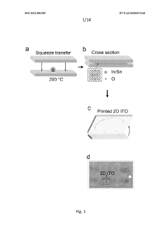
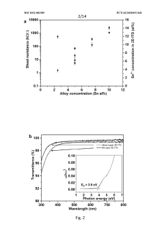
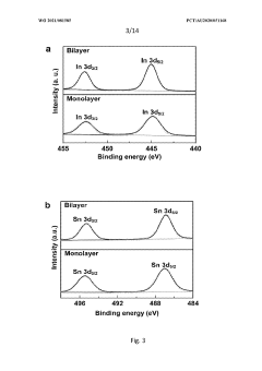
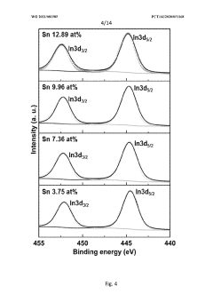
- The development of a method to form thin, flexible ternary metal oxide coatings using a liquid indium-tin alloy that oxidizes in ambient conditions, creating a monolayer or bilayer of indium tin oxide with a thickness of less than 50 nm, offering high conductivity and transparency while reducing the need for vacuum processing and indium usage.
Sustainability Aspects of TCO Materials
The sustainability of Transparent Conductive Oxide (TCO) materials has become increasingly important as printed electronics gain wider adoption across various industries. Environmental considerations now play a crucial role in material selection and manufacturing processes for TCOs, with regulatory frameworks worldwide pushing for greener alternatives.
Traditional TCO production methods often involve energy-intensive processes and the use of scarce elements like indium, raising significant sustainability concerns. The mining and processing of indium, a key component in Indium Tin Oxide (ITO), generates substantial environmental impacts including habitat destruction, water pollution, and high carbon emissions. Recent life cycle assessments indicate that the production of one kilogram of ITO can generate up to 150 kg of CO2 equivalent emissions.
Alternative TCO materials are emerging as more sustainable options. Fluorine-doped Tin Oxide (FTO) and Aluminum-doped Zinc Oxide (AZO) utilize more abundant elements, reducing resource depletion concerns. These alternatives typically require 30-40% less energy during manufacturing compared to conventional ITO production methods. Additionally, novel carbon-based conductive materials like graphene and carbon nanotubes offer promising sustainability profiles with potentially lower environmental footprints.
Manufacturing innovations are also addressing sustainability challenges in TCO production. Low-temperature solution processing techniques compatible with printed electronics significantly reduce energy consumption compared to traditional vacuum deposition methods. Roll-to-roll manufacturing processes further enhance material efficiency by minimizing waste and enabling larger-scale production with reduced environmental impact per unit area.
End-of-life considerations represent another critical sustainability aspect for TCO materials. Recyclability varies significantly among different TCO formulations, with some newer compositions designed specifically for easier recovery and reuse. Closed-loop systems are being developed to reclaim valuable elements from discarded electronic devices containing TCOs, though implementation remains limited in commercial settings.
Economic sustainability must be balanced with environmental concerns. While some alternative TCOs offer improved ecological profiles, their production costs and performance characteristics may not yet match traditional options. This creates a complex decision matrix for manufacturers weighing immediate economic factors against long-term environmental sustainability. Industry consortiums are increasingly developing sustainability metrics specifically for transparent conductors to standardize evaluation across different material systems.
Future research directions in sustainable TCO development include bio-inspired materials, water-based processing methods, and designs that facilitate disassembly and material recovery. These innovations aim to address the full lifecycle environmental impact of TCO materials while maintaining the performance requirements essential for printed electronics applications.
Manufacturing Scalability Challenges
The scaling of transparent conductive oxide (TCO) manufacturing processes presents significant challenges that must be addressed for widespread adoption in printed electronics. Current deposition methods such as sputtering, chemical vapor deposition, and sol-gel processes face considerable hurdles when transitioning from laboratory to industrial scale production.
Material consistency represents a primary concern, as maintaining uniform electrical and optical properties across large substrate areas remains difficult. Variations in thickness, crystallinity, and defect concentration can lead to inconsistent performance in the final devices. This challenge is particularly pronounced when scaling up from small research samples to commercial-sized substrates that may span several square meters.
Process throughput limitations also constrain industrial adoption. Many high-quality TCO deposition techniques require vacuum environments or precise temperature control, resulting in slow processing speeds incompatible with high-volume manufacturing demands. The capital equipment costs for these precision systems further compound economic feasibility issues.
Energy consumption during manufacturing presents another significant barrier. Traditional TCO deposition methods often require high temperatures (300-600°C) for proper film formation and crystallization. These energy-intensive processes increase production costs and limit compatibility with temperature-sensitive flexible substrates crucial for next-generation printed electronics.
Material utilization efficiency remains suboptimal in many deposition techniques. Sputtering processes, for example, typically achieve only 30-40% material utilization, with the remainder becoming waste. This inefficiency increases production costs and creates environmental concerns, particularly when using indium-based TCOs given indium's limited natural abundance.
Integration challenges with existing manufacturing lines further complicate scalability. Many printed electronics applications require TCO deposition to seamlessly integrate with other process steps in roll-to-roll or sheet-to-sheet production environments. Current deposition technologies often create bottlenecks that disrupt continuous manufacturing workflows.
Quality control and process monitoring systems need significant development for industrial-scale TCO production. Real-time measurement of critical parameters such as sheet resistance, transparency, and film thickness across large areas remains technically challenging but essential for maintaining consistent product quality in high-volume manufacturing scenarios.
Unlock deeper insights with Patsnap Eureka Quick Research — get a full tech report to explore trends and direct your research. Try now!
Generate Your Research Report Instantly with AI Agent
Supercharge your innovation with Patsnap Eureka AI Agent Platform!