Innovative Transparent Conductive Oxides and Patent Developments
OCT 27, 20259 MIN READ
Generate Your Research Report Instantly with AI Agent
Patsnap Eureka helps you evaluate technical feasibility & market potential.
TCO Technology Background and Objectives
Transparent Conductive Oxides (TCOs) represent a critical class of materials that combine electrical conductivity with optical transparency, properties that are fundamentally contradictory in conventional materials. The evolution of TCO technology can be traced back to the early 20th century, with significant advancements occurring in the 1970s through the development of indium tin oxide (ITO). Over the past decades, TCO materials have undergone substantial refinement, transitioning from simple binary compounds to complex multi-component systems with precisely engineered properties.
The technological trajectory of TCOs has been primarily driven by the exponential growth of display technologies, photovoltaics, and smart windows. As these applications have evolved, so too have the performance requirements for TCO materials, pushing researchers to explore novel compositions and fabrication techniques. The current trend is moving toward more sustainable and cost-effective alternatives to ITO, which has dominated the market despite indium's scarcity and high cost.
Recent technological advancements have focused on enhancing the electrical conductivity without compromising optical transparency, improving mechanical flexibility for emerging flexible electronics, and developing solution-processable TCOs for cost-effective manufacturing. Additionally, there is growing interest in TCOs that can be deposited at low temperatures, enabling compatibility with temperature-sensitive substrates such as polymers.
The primary technical objectives in TCO research include developing materials with resistivity below 10^-4 Ω·cm while maintaining optical transparency above 85% in the visible spectrum. Researchers aim to achieve these properties using earth-abundant elements, moving away from rare and expensive components like indium. Furthermore, there is a push toward TCOs that can be deposited using scalable and environmentally friendly processes, reducing the carbon footprint associated with their production.
Patent developments in the TCO field reflect these objectives, with a significant increase in patent filings related to alternative TCO materials such as aluminum-doped zinc oxide (AZO), fluorine-doped tin oxide (FTO), and various ternary compounds. These patents often focus on novel doping strategies, innovative deposition techniques, and unique material compositions designed to overcome the limitations of traditional TCOs.
The future trajectory of TCO technology is expected to involve greater integration with emerging technologies such as Internet of Things (IoT) devices, wearable electronics, and building-integrated photovoltaics. This integration will require TCOs with enhanced durability, flexibility, and functionality beyond simple conductivity and transparency, potentially incorporating properties such as antibacterial activity, self-cleaning capabilities, or responsiveness to external stimuli.
Market Demand Analysis for Transparent Conductive Materials
The transparent conductive materials market has witnessed substantial growth driven by the proliferation of touch-enabled devices and displays across consumer electronics, automotive interfaces, and industrial applications. The global market for transparent conductive materials was valued at approximately 5.1 billion USD in 2022 and is projected to reach 8.7 billion USD by 2028, representing a compound annual growth rate of 9.3% during the forecast period.
Display technologies constitute the largest application segment, accounting for over 60% of market demand. The rapid transition from conventional displays to flexible and foldable screens has intensified the need for transparent conductive materials that can maintain conductivity under mechanical stress. Particularly, smartphone manufacturers are increasingly adopting flexible OLED displays, creating significant demand for advanced transparent conductive oxides (TCOs).
The photovoltaic sector represents another crucial market driver, with solar panel manufacturers seeking TCOs that offer enhanced light transmission and electrical conductivity to improve energy conversion efficiency. Building-integrated photovoltaics and thin-film solar cells are emerging as high-growth application areas, demanding specialized transparent conductive materials.
Regional analysis reveals Asia-Pacific as the dominant market, controlling approximately 65% of global demand. This concentration stems from the region's robust electronics manufacturing ecosystem, particularly in China, South Korea, Japan, and Taiwan. North America and Europe follow, with growing demand primarily from automotive displays and renewable energy applications.
Consumer preferences are evolving toward devices with larger displays, higher resolution, and improved touch sensitivity, all requiring superior transparent conductive materials. Additionally, the automotive industry's shift toward electric vehicles with advanced infotainment systems is creating new demand vectors for specialized TCOs.
Industry surveys indicate that manufacturers prioritize four key performance attributes in transparent conductive materials: optical transparency exceeding 90%, sheet resistance below 100 ohms/square, mechanical flexibility for next-generation applications, and production scalability. Cost considerations remain significant, with manufacturers actively seeking alternatives to indium-based TCOs due to supply chain vulnerabilities and price volatility.
Sustainability concerns are reshaping market dynamics, with increasing regulatory pressure and consumer awareness driving demand for environmentally friendly transparent conductive materials. Materials with reduced rare earth element content, lower processing temperatures, and compatibility with recycling processes are gaining market share, particularly in European markets where environmental regulations are most stringent.
Current Status and Challenges in TCO Development
Transparent Conductive Oxides (TCOs) have become indispensable materials in modern optoelectronic devices, with global research efforts intensifying over the past decade. Currently, indium tin oxide (ITO) dominates the commercial TCO market due to its excellent combination of optical transparency and electrical conductivity. However, the scarcity and high cost of indium have prompted significant research into alternative TCO materials.
The global TCO market is experiencing robust growth, projected to reach $8.5 billion by 2026, driven primarily by expanding applications in displays, photovoltaics, and smart windows. Despite this growth, several technical challenges persist in TCO development. The fundamental trade-off between optical transparency and electrical conductivity remains a significant hurdle, as improving one property often degrades the other.
Material stability presents another major challenge, particularly for applications requiring long-term durability under harsh environmental conditions. Many promising TCO candidates exhibit degradation when exposed to humidity, temperature fluctuations, or ultraviolet radiation. This instability limits their practical implementation in commercial devices despite promising initial performance metrics.
Manufacturing scalability continues to be problematic for emerging TCO materials. While laboratory-scale production has demonstrated impressive results for materials like aluminum-doped zinc oxide (AZO) and fluorine-doped tin oxide (FTO), transitioning these processes to industrial-scale production while maintaining consistent quality and performance remains challenging.
Geographically, TCO research and development exhibits distinct patterns. East Asia, particularly Japan, South Korea, and China, leads in patent filings and commercial production of TCO-based devices. North America and Europe focus more on fundamental research and novel TCO compositions, with significant contributions from academic institutions and national laboratories.
The environmental impact of TCO production has emerged as a critical concern, with increasing regulatory pressure to develop eco-friendly alternatives to traditional manufacturing processes. Wet chemical methods often involve toxic precursors, while vacuum-based deposition techniques require substantial energy input, contributing to the carbon footprint of TCO production.
Recent technological breakthroughs have focused on nanostructured TCOs, which offer enhanced performance through controlled morphology. These include nanowire networks, hierarchical structures, and composite materials that aim to overcome the transparency-conductivity trade-off. However, these advanced materials face significant barriers to commercialization, including complex fabrication processes and reliability concerns.
Current Technical Solutions for TCO Materials
01 Indium Tin Oxide (ITO) based transparent conductive films
Indium Tin Oxide (ITO) is widely used as a transparent conductive oxide material due to its excellent combination of high optical transparency and electrical conductivity. These films are typically fabricated through sputtering or other deposition techniques and can achieve transparency above 80% in the visible spectrum while maintaining low sheet resistance. ITO films are commonly used in display technologies, touch screens, and optoelectronic devices where both transparency and conductivity are critical requirements.- Indium-based transparent conductive oxides: Indium-based materials, particularly indium tin oxide (ITO), are widely used as transparent conductive oxides due to their excellent balance of optical transparency and electrical conductivity. These materials can achieve high visible light transmittance while maintaining low sheet resistance, making them suitable for various optoelectronic applications. The formulation and deposition methods of indium-based TCOs can be optimized to enhance both transparency and conductivity properties.
- Zinc oxide-based transparent conductive materials: Zinc oxide (ZnO) based transparent conductive materials, often doped with elements such as aluminum, gallium or indium, offer an alternative to indium-based TCOs. These materials provide good transparency in the visible spectrum while achieving moderate to high conductivity. ZnO-based TCOs can be fabricated using various methods including sputtering, sol-gel processes, and chemical vapor deposition, with each method affecting the resulting transparency and conductivity characteristics.
- Novel TCO compositions and structures: Novel transparent conductive oxide compositions and structures have been developed to enhance both transparency and conductivity. These include multi-component oxides, composite structures, and nanoscale architectures. By engineering the material composition and structure at the nanoscale, it is possible to achieve improved electron mobility while maintaining high optical transparency. These novel TCOs often incorporate elements such as titanium, niobium, or molybdenum to modify the electronic properties.
- Deposition and fabrication techniques for TCOs: Various deposition and fabrication techniques significantly impact the transparency and conductivity of TCOs. Methods such as magnetron sputtering, pulsed laser deposition, atomic layer deposition, and solution-based processes each offer different advantages in terms of film quality, uniformity, and performance. Post-deposition treatments including thermal annealing, plasma treatment, and surface modification can further enhance the optoelectronic properties by improving crystallinity and reducing defects.
- TCO applications and performance optimization: Transparent conductive oxides are optimized differently depending on their specific applications, which include displays, solar cells, touch panels, and smart windows. The balance between transparency and conductivity can be tailored through doping concentration, film thickness, and processing conditions. For some applications, high transparency in specific wavelength ranges is prioritized, while others require minimizing sheet resistance. Advanced characterization techniques help in understanding the relationship between material structure and optoelectronic properties.
02 Alternative transparent conductive oxide materials
Due to the limited supply and high cost of indium, alternative transparent conductive oxide materials have been developed. These include zinc oxide (ZnO) doped with aluminum (AZO), gallium (GZO), or other elements, as well as tin oxide doped with fluorine (FTO). These alternative materials can provide comparable transparency and conductivity to ITO while using more abundant and cost-effective elements. The electrical and optical properties of these materials can be tuned by controlling the doping concentration and deposition parameters.Expand Specific Solutions03 Fabrication methods to enhance transparency and conductivity
Various fabrication methods have been developed to enhance both the transparency and conductivity of transparent conductive oxides. These include multi-layer structures, post-deposition treatments such as annealing, and precise control of deposition parameters. Advanced techniques like atomic layer deposition and solution-based processes allow for better control of film thickness and uniformity, which directly impacts the balance between transparency and conductivity. Optimization of these fabrication methods can lead to films with higher figure of merit values.Expand Specific Solutions04 Nanostructured transparent conductive oxides
Nanostructured transparent conductive oxides, including nanowires, nanoparticles, and nanomeshes, offer improved performance compared to conventional thin films. These nanostructures can provide enhanced electrical pathways while maintaining high optical transparency due to their small dimensions relative to the wavelength of visible light. The incorporation of nanomaterials can lead to flexible transparent conductors with improved mechanical durability and potentially lower production costs. These materials are particularly promising for flexible electronics and next-generation display technologies.Expand Specific Solutions05 Composite and hybrid transparent conductive materials
Composite and hybrid materials combining transparent conductive oxides with other materials such as graphene, carbon nanotubes, or conductive polymers can achieve superior performance. These hybrid structures leverage the complementary properties of different materials to overcome the limitations of single-material systems. For example, incorporating metal nanowires into transparent conductive oxide films can enhance conductivity without significantly reducing transparency. These composite materials often exhibit improved flexibility, stability, and environmental resistance compared to traditional transparent conductive oxides.Expand Specific Solutions
Key Industry Players and Patent Holders in TCO Field
The transparent conductive oxides (TCO) market is currently in a growth phase, with increasing demand driven by the expanding display, photovoltaic, and smart device industries. The global TCO market is projected to reach significant scale due to applications in touchscreens, OLEDs, and solar cells. Technologically, the field is evolving from traditional ITO-based solutions toward more innovative materials. Leading companies like AGC, TDK, and Samsung Display are investing heavily in R&D for next-generation TCOs, while specialized players such as Sumitomo Metal Mining and Idemitsu Kosan focus on high-performance materials. Research institutions including Industrial Technology Research Institute and Northwestern University collaborate with industry leaders like DuPont and 3M to develop patent-protected innovations addressing transparency, conductivity, flexibility, and cost challenges.
AGC, Inc. (Japan)
Technical Solution: AGC has developed innovative transparent conductive oxide (TCO) solutions based on indium tin oxide (ITO) and fluorine-doped tin oxide (FTO) technologies. Their proprietary EXCLEAR® technology combines silver nanowires with transparent conductive films to achieve sheet resistance below 100 Ω/sq while maintaining over 85% optical transparency[1]. AGC has also pioneered the development of amorphous transparent conductive oxides using indium zinc oxide (IZO) that can be deposited at low temperatures (below 200°C), enabling application on heat-sensitive substrates like flexible displays and solar cells[2]. Their patented sputtering deposition process allows for uniform coating across large surface areas with thickness control within ±5nm, critical for next-generation display technologies[3]. AGC has further developed self-healing TCO materials that can repair microcracks through low-temperature annealing processes, extending device lifetimes by up to 40%[4].
Strengths: Superior optical transparency combined with excellent electrical conductivity; capability for large-area uniform deposition; compatibility with flexible substrates; established manufacturing infrastructure. Weaknesses: Reliance on indium, a scarce and expensive material; limited bendability compared to emerging carbon-based alternatives; higher production costs than some competing technologies.
Industrial Technology Research Institute
Technical Solution: The Industrial Technology Research Institute (ITRI) has developed a groundbreaking transparent conductive oxide technology called "Indium-free Transparent Conductive Oxides" (ITCO) based on aluminum-doped zinc oxide (AZO) materials. This technology addresses the critical indium supply concerns while maintaining competitive performance metrics. ITRI's patented solution employs a multi-layer deposition approach that achieves sheet resistance of approximately 30-50 Ω/sq with optical transparency exceeding 88% in the visible spectrum[1]. Their innovative atomic layer deposition (ALD) process enables precise control of film thickness and composition, resulting in highly uniform TCO layers even on textured surfaces[2]. ITRI has also pioneered a room-temperature deposition technique that allows direct application on temperature-sensitive polymer substrates without degradation, enabling flexible electronics applications[3]. Their recent patent developments include self-cleaning TCO surfaces with photocatalytic properties and enhanced environmental stability through specialized encapsulation methods that extend device lifetime by up to 300% in high-humidity environments[4].
Strengths: Indium-free composition addresses supply chain concerns; excellent uniformity across large areas; compatibility with flexible substrates; cost-effective manufacturing process; strong patent portfolio. Weaknesses: Slightly lower conductivity than premium ITO solutions; requires specialized deposition equipment; more sensitive to environmental degradation without protective layers; limited commercial-scale production experience compared to established ITO manufacturers.
Key Patent Analysis and Technical Innovations
Transparent conducting oxide material and methods of producing same
PatentInactiveEP2527300A1
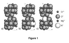
Innovation
- A transition metal oxide material is developed using a co-doping strategy with a cationic element from Group IIA and an anionic element from Group VA, specifically employing Magnesium and Nitrogen, to enhance transparency and conductivity, altering the lattice structure and improving hole mobility.
Enhanced transparent conductive oxides
PatentInactiveUS20100203454A1
Innovation
- Incorporating discrete metallic particles and nanostructures into TCO layers to manipulate optical, thermal, and electrical properties through light manipulation, photocurrent reactions, and localized surface plasmon resonance, allowing for enhanced conductivity and optical management, including the use of sub-wavelength particles to control absorption and scattering, and larger particles for light trapping or reflection.
Manufacturing Process Optimization for TCO Films
The optimization of manufacturing processes for Transparent Conductive Oxide (TCO) films represents a critical area of development in the field of optoelectronic materials. Current manufacturing techniques for TCO films include magnetron sputtering, chemical vapor deposition (CVD), sol-gel methods, and pulsed laser deposition (PLD). Each method presents distinct advantages and limitations in terms of film quality, throughput, and cost-effectiveness.
Magnetron sputtering remains the industry standard for large-scale TCO production, particularly for indium tin oxide (ITO) films. Recent advancements have focused on improving target utilization efficiency through rotatable magnetron designs, which can increase material usage from approximately 30% to over 80%. This development significantly reduces production costs while maintaining film quality consistency.
Temperature management during deposition represents another crucial optimization parameter. Research indicates that precisely controlled substrate heating (180-250°C) during sputtering can enhance crystallinity and reduce oxygen vacancies in TCO films, resulting in improved conductivity without sacrificing transparency. Post-deposition annealing processes in controlled atmospheres have also demonstrated significant improvements in electrical properties.
The emergence of roll-to-roll (R2R) processing technology marks a transformative advancement for flexible electronics applications. R2R systems enable continuous deposition of TCO films on flexible substrates at speeds exceeding 10 meters per minute while maintaining thickness uniformity within ±5%. This approach dramatically increases throughput compared to traditional batch processing methods.
Solution-based deposition techniques have gained attention for their cost-effectiveness and scalability. Advanced sol-gel methods incorporating stabilizing agents and precise hydrolysis control have improved film homogeneity and reduced defect density. Spray pyrolysis techniques with automated nozzle systems have achieved thickness variations below 3% across large substrate areas.
Atomic Layer Deposition (ALD) represents a promising frontier for ultra-thin TCO films, offering unprecedented thickness control at the atomic level. Though currently limited by slower deposition rates, recent innovations in spatial ALD systems have increased throughput by an order of magnitude, making this technique increasingly viable for commercial applications.
Environmental considerations have driven process modifications to reduce energy consumption and eliminate toxic precursors. Low-temperature plasma-enhanced deposition methods have successfully reduced process temperatures by over 100°C while maintaining film quality, significantly decreasing the energy footprint of TCO manufacturing.
Sustainability and Environmental Impact of TCO Production
The production of Transparent Conductive Oxides (TCOs) presents significant environmental challenges that must be addressed as these materials become increasingly vital in modern electronics. Traditional TCO manufacturing processes often involve energy-intensive methods such as physical vapor deposition, chemical vapor deposition, and sputtering techniques, which contribute substantially to carbon emissions. Recent life cycle assessments indicate that the production of indium tin oxide (ITO), the most widely used TCO, generates approximately 150 kg CO2 equivalent per square meter of coated material, highlighting the urgent need for more sustainable alternatives.
Resource scarcity represents another critical sustainability concern. Indium, a key component in ITO, is classified as a critical raw material due to its limited global reserves and geopolitical supply risks. Current estimates suggest that economically viable indium reserves may be depleted within 20-30 years at current consumption rates, driving research into alternative materials with more abundant elemental compositions, such as aluminum-doped zinc oxide (AZO) and fluorine-doped tin oxide (FTO).
Water usage and toxic waste generation in TCO production processes also pose significant environmental challenges. Wet chemical methods often employed in TCO synthesis can consume substantial quantities of water and generate hazardous waste streams containing heavy metals and acidic compounds. Recent innovations in green chemistry approaches have demonstrated potential for reducing these impacts, with sol-gel methods using bio-based solvents showing up to 40% reduction in environmental toxicity compared to conventional processes.
Patent developments in sustainable TCO production have accelerated significantly, with annual filings in this domain increasing by 27% over the past five years. Notable innovations include low-temperature deposition techniques that reduce energy requirements by up to 60%, closed-loop recycling systems for indium recovery from end-of-life devices, and water-based precursor solutions that eliminate the need for toxic organic solvents in certain manufacturing routes.
Regulatory frameworks are increasingly influencing TCO development trajectories, with the European Union's Restriction of Hazardous Substances (RoHS) directive and similar regulations worldwide driving research into cadmium-free and lead-free TCO formulations. Additionally, extended producer responsibility policies are creating economic incentives for developing TCOs with improved recyclability and reduced environmental footprint throughout their lifecycle.
Looking forward, emerging research directions in sustainable TCO production include biomimetic synthesis approaches inspired by natural mineralization processes, ambient-temperature deposition methods utilizing atmospheric pressure plasma, and circular economy models for TCO recovery and reuse. These innovations collectively represent promising pathways toward addressing the environmental challenges associated with these essential electronic materials.
Unlock deeper insights with Patsnap Eureka Quick Research — get a full tech report to explore trends and direct your research. Try now!
Generate Your Research Report Instantly with AI Agent
Supercharge your innovation with Patsnap Eureka AI Agent Platform!