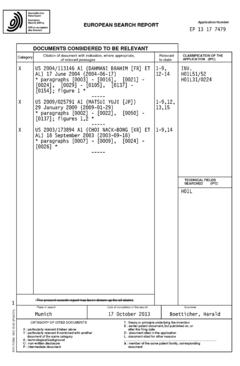
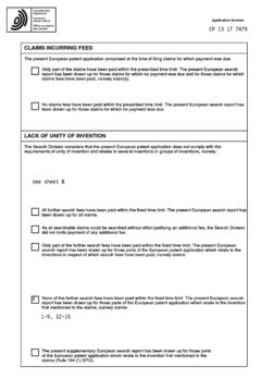
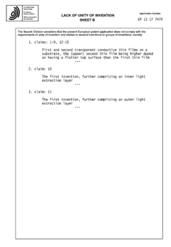
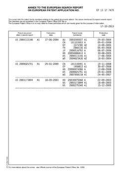
Transparent Conductive Oxides in the Electronics Industry
OCT 27, 20259 MIN READ
Generate Your Research Report Instantly with AI Agent
Patsnap Eureka helps you evaluate technical feasibility & market potential.
TCO Evolution and Research Objectives
Transparent Conductive Oxides (TCOs) have evolved significantly since their initial discovery in the early 20th century. The journey began with the identification of cadmium oxide (CdO) as a transparent conductor in 1907, followed by the development of tin oxide (SnO2) in the 1940s. The breakthrough came in the 1970s with the introduction of indium tin oxide (ITO), which revolutionized the electronics industry by offering an unprecedented combination of optical transparency and electrical conductivity.
The evolution of TCOs has been driven by the exponential growth of display technologies, photovoltaics, and touch-sensitive devices. Initially focused on improving transparency and conductivity, research objectives have expanded to address sustainability concerns, material scarcity, and manufacturing scalability. The critical shortage of indium, a key component in ITO, has accelerated research into alternative TCO materials over the past decade.
Current technological trends indicate a shift toward more abundant and environmentally friendly materials. Zinc oxide (ZnO) based compounds, fluorine-doped tin oxide (FTO), and aluminum-doped zinc oxide (AZO) have emerged as promising alternatives. Additionally, the integration of TCOs with emerging technologies such as flexible electronics and wearable devices has introduced new performance requirements, including mechanical flexibility and stability under bending conditions.
The primary research objectives in the TCO field now encompass several dimensions. First, developing indium-free or indium-reduced TCOs with comparable or superior performance to ITO remains a top priority. Second, enhancing the electrical conductivity while maintaining high optical transparency continues to challenge researchers, as these properties typically exhibit inverse relationships. Third, improving the mechanical flexibility and durability of TCOs for next-generation flexible displays and electronics represents a critical frontier.
Furthermore, research aims to develop cost-effective and environmentally sustainable manufacturing processes for TCO deposition. Traditional vacuum-based techniques like sputtering are being complemented by solution-based approaches that promise lower energy consumption and reduced production costs. The scalability of these processes for large-area applications presents both challenges and opportunities.
Looking forward, the convergence of TCO research with nanotechnology offers exciting possibilities. Nanostructured TCOs, composite materials, and hybrid organic-inorganic systems are being explored to overcome the fundamental limitations of conventional materials. The ultimate goal is to develop TCOs that can be tailored for specific applications while meeting increasingly stringent performance, sustainability, and cost requirements in the rapidly evolving electronics industry.
Market Analysis for Transparent Conductive Materials
The transparent conductive materials market has witnessed substantial growth in recent years, primarily driven by the expanding electronics industry and increasing demand for touchscreen devices. The global market for transparent conductive materials was valued at approximately $5.1 billion in 2022 and is projected to reach $8.3 billion by 2027, growing at a CAGR of 10.2% during the forecast period.
Indium Tin Oxide (ITO) continues to dominate the market with over 70% market share due to its excellent combination of optical transparency and electrical conductivity. However, the limited availability of indium and its rising cost have created significant market opportunities for alternative materials such as silver nanowires, carbon nanotubes, graphene, PEDOT:PSS, and metal mesh technologies.
The display panel segment represents the largest application area, accounting for nearly 60% of the market share. Smartphones and tablets collectively constitute approximately 45% of the end-use market, followed by LCD/LED displays (25%), touch panels (15%), and solar photovoltaics (10%). The remaining 5% is distributed among emerging applications including smart windows, OLED lighting, and flexible electronics.
Regionally, Asia-Pacific dominates the market with over 65% share, primarily due to the concentration of electronics manufacturing in countries like China, South Korea, Japan, and Taiwan. North America and Europe follow with approximately 15% and 12% market shares respectively, while emerging markets in Latin America and Middle East & Africa collectively account for the remaining 8%.
Key market drivers include the proliferation of touchscreen devices, growing demand for flexible electronics, increasing adoption of OLED displays, and expanding applications in the automotive sector for displays and smart windows. The push toward sustainable and energy-efficient technologies has also boosted demand for transparent conductors in solar cells and smart windows.
Market challenges include price volatility of raw materials, particularly indium, technical limitations in flexibility and durability for next-generation devices, and manufacturing scalability issues for newer alternative materials. The industry is also facing pressure to develop solutions that meet increasingly stringent environmental regulations regarding the use of rare earth elements.
Consumer electronics remains the primary end-user segment, but automotive and architectural applications are showing the fastest growth rates at 15.3% and 13.7% CAGR respectively. This diversification of application areas is expected to reshape market dynamics over the next five years, creating new opportunities for material innovations and specialized product offerings.
Current TCO Technologies and Challenges
Transparent Conductive Oxides (TCOs) currently dominate the transparent electrode market, with Indium Tin Oxide (ITO) being the most widely deployed solution. ITO combines high optical transparency (>85% in visible spectrum) with low electrical resistivity (approximately 10^-4 Ω·cm), making it ideal for applications in displays, touch panels, and photovoltaics. The industry standard deposition methods include magnetron sputtering, which offers excellent uniformity for large-area applications, and pulsed laser deposition for specialized research applications.
Despite ITO's commercial success, it faces significant challenges. The scarcity of indium, classified as a critical raw material, has led to price volatility and supply chain concerns. Current global indium reserves are estimated to last only 20-30 years at current consumption rates, necessitating alternatives. Additionally, ITO's brittleness limits its application in flexible electronics, as it develops microcracks under bending stress, rapidly degrading conductivity after repeated flexing cycles.
Alternative TCO materials have emerged to address these limitations. Fluorine-doped Tin Oxide (FTO) offers superior thermal stability and lower cost but exhibits higher resistivity than ITO. Aluminum-doped Zinc Oxide (AZO) presents a cost-effective alternative with comparable optical properties but suffers from moisture sensitivity and degradation in humid environments. Gallium-doped Zinc Oxide (GZO) demonstrates improved stability over AZO but remains less conductive than premium ITO.
Manufacturing challenges persist across all TCO technologies. High-temperature processing requirements (typically 300-400°C) limit compatibility with temperature-sensitive substrates. Achieving uniform electrical properties over large areas remains difficult, with edge effects and thickness variations causing performance inconsistencies. The trade-off between transparency and conductivity continues to be a fundamental constraint, as increasing carrier concentration improves conductivity but reduces optical transparency due to free carrier absorption.
Recent technological innovations focus on low-temperature deposition methods, including room-temperature sputtering with post-deposition treatments and solution-based processing routes. Atomic Layer Deposition (ALD) has shown promise for producing highly conformal TCO films with precise thickness control, though throughput limitations hinder industrial adoption. Compositional engineering through multi-component doping strategies has demonstrated potential for optimizing the transparency-conductivity balance.
The industry is increasingly demanding TCOs with specialized properties beyond basic conductivity and transparency. These include work function tunability for improved charge extraction in optoelectronic devices, enhanced chemical stability for harsh environment applications, and compatibility with flexible substrates for next-generation electronics. Meeting these diverse requirements while maintaining cost-effectiveness represents the central challenge for current TCO technologies.
Contemporary TCO Material Solutions
01 Composition and structure of transparent conductive oxides
Transparent conductive oxides (TCOs) are materials that combine electrical conductivity with optical transparency. These materials typically consist of metal oxides doped with specific elements to enhance their electrical properties while maintaining transparency. Common TCO compositions include indium tin oxide (ITO), zinc oxide (ZnO), and tin oxide (SnO2). The crystalline structure and composition significantly influence the performance characteristics of these materials, making them suitable for various electronic and optoelectronic applications.- Indium-based transparent conductive oxides: Indium-based materials, particularly indium tin oxide (ITO), are widely used as transparent conductive oxides due to their excellent combination of optical transparency and electrical conductivity. These materials are commonly employed in various electronic devices such as displays, touch screens, and photovoltaic cells. Research focuses on improving deposition methods, reducing material costs, and enhancing performance characteristics like conductivity and transparency.
- Zinc oxide-based transparent conductive materials: Zinc oxide (ZnO) based transparent conductive materials, often doped with elements like aluminum or gallium, represent an important alternative to indium-based TCOs. These materials offer advantages including abundance of raw materials, environmental friendliness, and stability under hydrogen plasma. Various deposition techniques are employed to create ZnO films with optimized electrical and optical properties for applications in solar cells, displays, and optoelectronic devices.
- Fabrication methods for transparent conductive oxide films: Various fabrication methods are employed to produce transparent conductive oxide films with optimized properties. These include sputtering, chemical vapor deposition, sol-gel processes, and atomic layer deposition. Each method offers different advantages in terms of film quality, process temperature, scalability, and cost-effectiveness. Research focuses on developing techniques that can produce high-quality TCO films with precise control over thickness, composition, and microstructure.
- Novel TCO compositions and structures: Research on transparent conductive oxides extends beyond traditional materials to novel compositions and structures. This includes multi-component oxides, nanostructured materials, and composite systems that can offer improved performance or specific functionalities. These innovations aim to overcome limitations of conventional TCOs by enhancing conductivity while maintaining high transparency, improving flexibility, or adding new properties such as antibacterial activity or self-cleaning capabilities.
- Applications of transparent conductive oxides: Transparent conductive oxides find applications across numerous technological fields. They are essential components in touch screens, flat panel displays, smart windows, photovoltaic devices, and organic light-emitting diodes. Emerging applications include flexible electronics, wearable devices, and transparent heaters. The specific requirements for TCO properties vary depending on the application, driving research toward tailored materials with optimized characteristics for each use case.
02 Deposition methods for transparent conductive oxide films
Various deposition techniques are employed to create thin films of transparent conductive oxides on different substrates. These methods include sputtering, chemical vapor deposition (CVD), atomic layer deposition (ALD), and sol-gel processes. Each technique offers specific advantages in terms of film quality, uniformity, and scalability. The deposition parameters, such as temperature, pressure, and gas composition, significantly affect the electrical and optical properties of the resulting TCO films, allowing for customization based on application requirements.Expand Specific Solutions03 Applications of transparent conductive oxides in electronic devices
Transparent conductive oxides are widely used in various electronic and optoelectronic devices. They serve as essential components in touch screens, liquid crystal displays (LCDs), organic light-emitting diodes (OLEDs), and solar cells. In these applications, TCOs function as transparent electrodes that allow light to pass through while conducting electricity. The specific requirements for TCO properties vary depending on the application, with factors such as sheet resistance, transparency, and stability being critical considerations for device performance and longevity.Expand Specific Solutions04 Enhancement of transparent conductive oxide properties
Various methods are employed to enhance the properties of transparent conductive oxides, including doping, multilayer structures, and post-deposition treatments. Doping with elements such as aluminum, gallium, or fluorine can significantly improve electrical conductivity while maintaining optical transparency. Post-deposition treatments, including thermal annealing and plasma treatments, can optimize the crystalline structure and reduce defects. Additionally, creating composite or multilayer structures with other materials can lead to improved stability, flexibility, and overall performance of TCO-based devices.Expand Specific Solutions05 Novel transparent conductive oxide materials and fabrication techniques
Research in transparent conductive oxides focuses on developing novel materials and fabrication techniques to overcome limitations of traditional TCOs. This includes exploring alternative compositions such as amorphous oxide semiconductors, ternary compounds, and nanostructured materials. Advanced fabrication methods, including solution processing, printing techniques, and low-temperature deposition, are being investigated to enable TCO integration with flexible and temperature-sensitive substrates. These innovations aim to address challenges related to material scarcity, cost, flexibility, and environmental impact while maintaining or improving electrical and optical performance.Expand Specific Solutions
Leading Companies and Research Institutions in TCO Field
The transparent conductive oxides (TCO) market in the electronics industry is currently in a growth phase, with increasing demand driven by applications in displays, photovoltaics, and touch panels. The global market size is expanding rapidly, projected to reach significant value due to rising adoption in consumer electronics and renewable energy sectors. Technologically, the field shows varying maturity levels, with established players like Samsung Electronics and LG Chem leading commercial applications, while research institutions such as IMEC and Oregon State University drive innovation. Companies including Eastman Kodak, TDK Corp, and Micron Technology are advancing material development, while AGC and Sumitomo Metal Mining focus on manufacturing scalability. The competitive landscape features collaboration between industrial giants and academic institutions to overcome challenges in transparency, conductivity, and cost-effectiveness.
Sumitomo Metal Mining Co. Ltd.
Technical Solution: Sumitomo Metal Mining has pioneered high-performance ITO target materials with superior uniformity and density characteristics. Their proprietary sintering process creates ITO targets with 99.99% density and controlled tin distribution, enabling consistent thin film deposition. Sumitomo has developed specialized TCO materials including zinc-tin oxide (ZTO) and gallium-doped zinc oxide (GZO) that offer improved etching properties and environmental stability. Their recent innovations include nanoparticle-based TCO inks for printed electronics applications, achieving sheet resistance of 50-100 ohms/square with over 85% transparency. Sumitomo's materials science expertise has led to TCO formulations that maintain performance under mechanical stress, critical for flexible display applications.
Strengths: World-class materials engineering capabilities; comprehensive supply chain control from raw materials to finished TCO products; extensive intellectual property portfolio. Weaknesses: Higher production costs compared to some competitors; primarily focused on materials rather than complete device solutions.
Samsung Electronics Co., Ltd.
Technical Solution: Samsung has developed advanced indium tin oxide (ITO) alternatives for flexible displays and touchscreens. Their proprietary metal oxide formulations include indium zinc oxide (IZO) and aluminum-doped zinc oxide (AZO) with enhanced flexibility and conductivity. Samsung's TCO technology features ultra-thin film deposition methods that maintain transparency above 90% while achieving sheet resistance below 10 ohms/square. Their solution-processed metal oxide semiconductors enable low-temperature fabrication compatible with flexible substrates. Samsung has integrated these TCOs into their commercial OLED displays, demonstrating scalable manufacturing techniques that maintain performance while reducing indium content by up to 30% compared to traditional ITO films.
Strengths: Vertical integration allowing direct implementation in consumer electronics; extensive manufacturing infrastructure; proven scalability. Weaknesses: Proprietary technologies limit broader industry adoption; still partially dependent on rare indium resources.
Key Patents and Scientific Breakthroughs in TCO Research
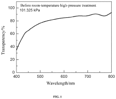
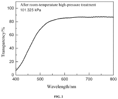
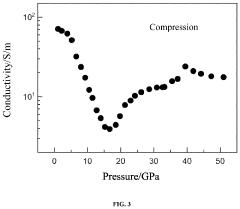
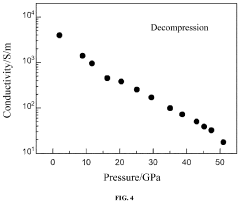
Method for improving conductivity and blue light filtering efficiency of transparent conducting oxide (TCO)
PatentActiveUS20240092650A1
Innovation
- A method involving room-temperature high-pressure treatment of indium oxide-based TCO materials, specifically titanium-doped indium oxide, which undergoes a structural phase transition from a cubic to a corundum structure, significantly enhancing conductivity and blue light filtering efficiency while maintaining high transparency.
Transparent conductive oxide thin film substrate, method of fabricating the same, and organic light-emitting device and photovoltaic cell having the same
PatentActiveEP2690683A3
Innovation
- A bi-layer transparent conductive oxide thin film substrate is fabricated using a base substrate with a first transparent conductive oxide thin film treated with a low concentration dopant, followed by a second thin film treated with a higher concentration dopant, achieving a smoother surface and reduced leakage current, and the process includes an inner and outer light extraction layer for enhanced performance.
Environmental Impact and Sustainability of TCO Materials
The environmental impact of Transparent Conductive Oxide (TCO) materials has become increasingly significant as electronics production scales globally. Traditional TCO manufacturing processes often involve energy-intensive methods and potentially hazardous materials, raising concerns about their overall sustainability. Indium Tin Oxide (ITO), the most widely used TCO, presents particular challenges due to the scarcity of indium, with reserves potentially facing depletion within decades at current consumption rates.
Manufacturing processes for TCOs typically require high temperatures and vacuum conditions, resulting in substantial energy consumption and associated carbon emissions. The sputtering techniques commonly employed for ITO deposition are particularly energy-intensive, with estimates suggesting that TCO layer production can account for up to 20% of the energy footprint in certain display manufacturing processes.
Chemical waste generation presents another environmental challenge. Etching processes used in TCO patterning often utilize acids and other hazardous chemicals that require careful handling and disposal. Improper management of these substances can lead to soil contamination and water pollution, particularly in regions with less stringent environmental regulations.
Recent sustainability initiatives have focused on developing alternative TCO materials with reduced environmental impact. Fluorine-doped Tin Oxide (FTO) and Aluminum-doped Zinc Oxide (AZO) represent promising alternatives that utilize more abundant elements. These materials can be deposited using less energy-intensive methods such as spray pyrolysis and sol-gel techniques, potentially reducing the carbon footprint of manufacturing processes by 30-40% compared to traditional ITO production.
Recycling and recovery systems for TCO materials are also advancing, though significant challenges remain. Current recovery rates for indium from end-of-life electronics remain below 1% globally, representing a substantial loss of this critical material. Improved recycling technologies and circular economy approaches are being developed to address this issue, with some pilot programs demonstrating recovery rates of up to 90% for indium from LCD panel waste.
Life cycle assessment (LCA) studies indicate that the environmental impact of TCOs extends beyond manufacturing to include extraction, processing, and end-of-life disposal. These analyses suggest that transitioning to more sustainable TCO alternatives could reduce the overall environmental footprint of electronic devices by 5-15%, depending on the specific application and implementation approach.
Industry standards and regulations are increasingly addressing the sustainability aspects of TCO materials. The European Union's Restriction of Hazardous Substances (RoHS) directive and similar regulations worldwide have pushed manufacturers to develop more environmentally friendly TCO formulations and processing methods, driving innovation in this field.
Manufacturing Processes and Scalability Considerations
The manufacturing processes for Transparent Conductive Oxides (TCOs) have evolved significantly over the past decades, with several techniques now established for industrial-scale production. Physical vapor deposition (PVD) methods, particularly magnetron sputtering, remain the dominant approach for TCO deposition due to their excellent uniformity and scalability. This process allows for precise control of film thickness and composition across large substrate areas, making it ideal for display manufacturing where consistency is paramount.
Chemical vapor deposition (CVD) techniques offer an alternative route with advantages in step coverage and the ability to coat complex geometries. Atmospheric pressure CVD has gained traction for its lower equipment costs, while plasma-enhanced CVD provides enhanced film quality at lower deposition temperatures. These methods are particularly valuable for flexible electronics applications where conformality over non-planar surfaces is required.
Solution-based deposition methods have emerged as cost-effective alternatives for certain applications. Techniques such as sol-gel processing, spray pyrolysis, and inkjet printing offer significant reductions in capital equipment costs and enable roll-to-roll manufacturing possibilities. However, these approaches typically yield TCO films with lower electrical performance compared to vacuum-based methods, limiting their application to less demanding products.
Scalability considerations present significant challenges for TCO manufacturing. The transition from laboratory to industrial production often reveals issues with process stability and yield rates. Large-area uniformity remains problematic, particularly for solution-based methods where thickness variations can compromise device performance. Additionally, the industry faces increasing pressure to reduce indium dependency in ITO (Indium Tin Oxide) production due to supply constraints and price volatility of this critical raw material.
Energy consumption represents another key scalability factor. Vacuum-based deposition techniques require substantial energy inputs, contributing significantly to production costs and environmental impact. Recent developments in low-temperature processing aim to address this concern, with room-temperature deposition methods showing promising results for certain TCO materials like aluminum-doped zinc oxide.
Equipment throughput and maintenance requirements further influence scalability economics. Modern in-line sputtering systems have dramatically improved production efficiency, but initial capital investments remain substantial. Meanwhile, solution-based approaches offer lower entry barriers but may incur higher operational costs due to material waste and quality control challenges. The optimal manufacturing approach ultimately depends on specific application requirements, production volume targets, and available infrastructure.
Unlock deeper insights with Patsnap Eureka Quick Research — get a full tech report to explore trends and direct your research. Try now!
Generate Your Research Report Instantly with AI Agent
Supercharge your innovation with Patsnap Eureka AI Agent Platform!