Analysis of Metal Oxide TFTs in Radiation-Resistant Electronics
SEP 28, 202510 MIN READ
Generate Your Research Report Instantly with AI Agent
Patsnap Eureka helps you evaluate technical feasibility & market potential.
Metal Oxide TFT Evolution and Radiation Hardening Goals
Metal oxide thin-film transistors (TFTs) have evolved significantly since their inception in the early 2000s, transforming from laboratory curiosities to commercially viable alternatives to silicon-based technologies. The evolution began with zinc oxide (ZnO) based devices, which demonstrated promising electron mobility but suffered from stability issues. A breakthrough came in 2004 when researchers at Tokyo Institute of Technology introduced indium gallium zinc oxide (IGZO), which offered superior stability and performance characteristics.
The technological trajectory continued with the development of various metal oxide semiconductors including zinc tin oxide (ZTO), indium zinc oxide (IZO), and hafnium indium zinc oxide (HIZO), each offering specific advantages in terms of mobility, transparency, and processing temperature requirements. These advancements enabled the expansion of TFT applications beyond traditional display technologies into flexible electronics, transparent circuits, and sensing devices.
Radiation hardening emerged as a critical research direction around 2010, when aerospace and nuclear industries recognized the potential of metal oxide TFTs for harsh environment applications. Initial radiation exposure studies revealed that metal oxide semiconductors exhibited inherently higher radiation tolerance compared to conventional silicon technologies, primarily due to their amorphous structure and wider bandgap characteristics.
The radiation hardening goals for metal oxide TFTs have evolved to address specific performance metrics under various radiation conditions. Primary objectives include maintaining threshold voltage stability under total ionizing dose (TID) exposure, minimizing leakage current increases, and preserving carrier mobility after radiation events. Quantitative targets typically specify functional operation after exposure to radiation doses ranging from 100 krad to 1 Mrad, depending on the application environment.
Current research focuses on enhancing radiation hardness through materials engineering approaches, including the incorporation of rare earth elements as dopants, optimization of oxygen vacancy concentrations, and development of multi-layer channel structures. These strategies aim to mitigate radiation-induced defect formation and charge trapping mechanisms that degrade device performance.
The technological roadmap for radiation-hardened metal oxide TFTs includes several ambitious goals: achieving operational stability at temperatures exceeding 200°C while under radiation exposure, developing devices capable of withstanding neutron fluences above 10^15 n/cm², and creating flexible radiation-hard electronics that maintain performance integrity under mechanical stress and radiation environments simultaneously.
Recent innovations point toward hybrid approaches that combine the inherent radiation tolerance of metal oxides with protective encapsulation layers and circuit-level redundancy techniques to create comprehensive radiation-hardened systems suitable for space exploration, nuclear power monitoring, and military applications.
Market Analysis for Radiation-Resistant Electronics
The radiation-resistant electronics market is experiencing significant growth driven by expanding applications in aerospace, defense, nuclear energy, and healthcare sectors. The global market for radiation-hardened electronics was valued at approximately $1.5 billion in 2022 and is projected to reach $2.2 billion by 2027, representing a compound annual growth rate of 7.8%. This growth trajectory is primarily fueled by increasing satellite deployments, space exploration missions, and modernization of nuclear facilities worldwide.
The aerospace and defense sectors currently dominate the market demand, accounting for over 60% of the total market share. With the commercialization of space and the rise of private space companies like SpaceX, Blue Origin, and numerous small satellite manufacturers, the demand for radiation-resistant components has expanded beyond traditional government and military applications. The commercial space sector alone is expected to drive a 12% annual increase in demand for radiation-hardened electronics through 2030.
Nuclear energy applications represent the second-largest market segment, with significant growth potential as countries invest in next-generation nuclear power plants and extend the operational life of existing facilities. The healthcare sector, particularly in radiation therapy equipment and medical imaging systems, constitutes an emerging market with projected growth rates exceeding 9% annually.
Geographically, North America leads the market with approximately 45% share, followed by Europe (25%) and Asia-Pacific (20%). However, the Asia-Pacific region is expected to witness the fastest growth rate due to increasing investments in space programs by countries like China, India, and Japan, along with expanding nuclear energy initiatives.
The market for Metal Oxide TFTs specifically within radiation-resistant electronics represents a high-growth niche segment. These components are gaining traction due to their superior performance characteristics in radiation environments compared to traditional silicon-based technologies. The market for Metal Oxide TFT-based radiation-resistant displays and sensors is estimated to grow at 14% annually, outpacing the broader market.
Customer requirements are increasingly focused on miniaturization, power efficiency, and enhanced radiation tolerance levels. End-users are demanding components that can withstand total ionizing doses exceeding 300 krad while maintaining operational stability. Additionally, there is growing interest in flexible and transparent radiation-resistant electronics for next-generation applications in wearable radiation monitors and advanced spacecraft instrumentation.
Price sensitivity varies significantly across market segments, with defense and space applications prioritizing performance over cost, while commercial applications demand more cost-effective solutions. This market dynamic is creating opportunities for tiered product strategies that address different performance-price requirements across various application domains.
Current Status and Challenges in Radiation-Hardened TFTs
Metal oxide thin-film transistors (TFTs) have emerged as promising candidates for radiation-resistant electronics due to their unique material properties and structural advantages. Currently, the global research landscape shows significant advancements in radiation-hardened TFTs, with major contributions from research institutions in the United States, Europe, and Asia. The development of these technologies has been accelerated by increasing demands from space exploration, nuclear energy, and military applications.
The state-of-the-art in radiation-hardened metal oxide TFTs demonstrates total ionizing dose (TID) tolerance exceeding 1 Mrad(Si) for optimized devices, representing a substantial improvement over conventional silicon-based technologies. Indium-gallium-zinc-oxide (IGZO) has emerged as the leading material system, with hafnium-indium-zinc-oxide (HIZO) and aluminum-doped zinc oxide (AZO) also showing promising radiation resistance characteristics.
Despite these advances, several critical challenges persist in the development of radiation-hardened TFTs. The primary technical obstacle remains the radiation-induced threshold voltage shift, which compromises device stability under prolonged radiation exposure. This phenomenon is attributed to charge trapping at the semiconductor-dielectric interface and within the gate dielectric itself, leading to performance degradation over time.
Another significant challenge is the trade-off between radiation hardness and electrical performance. Modifications that enhance radiation tolerance often result in reduced carrier mobility or increased off-state current, limiting the practical application of these devices in high-performance circuits. This balance between radiation resistance and electrical characteristics represents a fundamental design constraint that requires innovative solutions.
Manufacturing scalability presents another hurdle, as current fabrication techniques for high-performance radiation-hardened TFTs often involve complex processes that are difficult to implement in large-scale production. The integration of these devices with conventional CMOS technology also remains problematic, limiting their adoption in mixed-signal systems that could benefit from their radiation-resistant properties.
Temperature stability under radiation represents an additional challenge, as the combined effects of thermal stress and radiation exposure can lead to accelerated degradation mechanisms not observed under single-stress conditions. This synergistic effect complicates reliability predictions and requires comprehensive testing methodologies that account for realistic operational environments.
The development of accurate modeling and simulation tools specifically tailored for radiation effects in metal oxide semiconductors lags behind experimental advances, hampering predictive design capabilities. Current models often fail to capture the complex interaction between radiation-induced defects and charge transport mechanisms in these materials, necessitating extensive empirical testing.
Current Metal Oxide TFT Solutions for Radiation Environments
01 Radiation-resistant metal oxide semiconductor materials
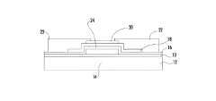
Metal oxide semiconductors such as indium gallium zinc oxide (IGZO) demonstrate inherent radiation resistance due to their wide bandgap and amorphous structure. These materials can maintain stable electrical characteristics when exposed to various types of radiation, making them suitable for applications in harsh radiation environments. The unique atomic bonding and defect states in these oxides contribute to their ability to withstand radiation damage without significant performance degradation.- Radiation-resistant metal oxide semiconductor materials: Metal oxide semiconductors, particularly those based on materials like indium gallium zinc oxide (IGZO), demonstrate inherent radiation resistance due to their wide bandgap and amorphous structure. These materials can maintain stable electrical characteristics even after exposure to various types of radiation, making them suitable for applications in harsh radiation environments. The radiation hardness of these materials can be further enhanced through specific composition optimization and processing techniques.
- Protective layer structures for radiation hardening: Implementing specialized protective layer structures can significantly enhance the radiation resistance of metal oxide TFTs. These structures include radiation-absorbing capping layers, buffer layers, and passivation films that shield the active semiconductor layer from radiation damage. Multi-layer protection schemes using combinations of organic and inorganic materials can effectively mitigate radiation-induced degradation while maintaining device performance characteristics.
- Circuit design techniques for radiation tolerance: Specialized circuit design methodologies can improve the radiation tolerance of metal oxide TFT-based systems. These include redundant transistor configurations, radiation-aware layout techniques, and compensation circuits that can adjust for radiation-induced threshold voltage shifts. Implementing feedback mechanisms and self-healing circuit architectures allows for dynamic adaptation to radiation effects, maintaining operational stability in high-radiation environments.
- Annealing and treatment processes for radiation hardening: Post-fabrication thermal annealing and specialized treatment processes can significantly enhance the radiation resistance of metal oxide TFTs. These processes include high-temperature annealing in controlled atmospheres, oxygen plasma treatments, and UV exposure techniques that stabilize the semiconductor microstructure. Such treatments can reduce oxygen vacancy concentrations and defect states that would otherwise serve as radiation-induced charge trapping sites, thereby improving overall radiation hardness.
- Doping strategies for enhanced radiation resistance: Strategic doping of metal oxide semiconductor materials with specific elements can enhance their radiation resistance properties. Incorporating elements such as hafnium, aluminum, or rare earth metals into the oxide semiconductor matrix can create more stable electronic structures that are less susceptible to radiation-induced displacement damage. These dopants can suppress the formation of oxygen vacancies during radiation exposure and provide additional charge compensation mechanisms that maintain device performance under radiation stress.
02 Structural modifications for enhanced radiation hardness
Specific structural modifications can be implemented in metal oxide TFTs to improve their radiation resistance. These include optimizing the gate dielectric interface, incorporating buffer layers, and modifying the channel thickness. Multi-layer structures with carefully engineered interfaces can reduce charge trapping and displacement damage caused by radiation. Additionally, specialized annealing processes can create more stable oxide structures that better withstand radiation effects.Expand Specific Solutions03 Doping strategies for radiation-hardened metal oxide TFTs
Strategic doping of metal oxide semiconductors can significantly enhance their radiation resistance. Introducing specific elements such as hafnium, titanium, or aluminum into the oxide matrix can create trap sites that capture radiation-induced charges, preventing their migration to critical device regions. Controlled doping concentrations can optimize the trade-off between radiation hardness and maintaining essential electrical performance characteristics like mobility and threshold voltage stability.Expand Specific Solutions04 Passivation and encapsulation techniques
Advanced passivation and encapsulation methods provide additional protection for metal oxide TFTs against radiation damage. Specialized passivation layers using silicon nitride, aluminum oxide, or organic-inorganic hybrid materials can prevent radiation-induced degradation by blocking particle penetration and reducing surface-related defect formation. Hermetic sealing techniques further isolate sensitive device components from environmental factors that could exacerbate radiation damage effects.Expand Specific Solutions05 Circuit design approaches for radiation-tolerant TFT systems
Circuit-level design strategies can complement material improvements to enhance overall radiation tolerance of metal oxide TFT systems. Redundant transistor configurations, radiation-aware layout techniques, and specialized biasing schemes can mitigate radiation effects at the system level. Implementing error correction mechanisms and radiation-tolerant peripheral circuits ensures reliable operation in radiation environments. These approaches often involve trade-offs between radiation hardness, power consumption, and circuit complexity.Expand Specific Solutions
Key Industry Players in Radiation-Hardened Electronics
The metal oxide TFT market for radiation-resistant electronics is currently in a growth phase, with increasing applications in aerospace, nuclear, and medical imaging sectors. The market is projected to expand significantly as demand for resilient electronics in harsh environments rises. Technologically, companies like BOE Technology, Applied Materials, and Samsung Display are leading innovation, with significant contributions from Semiconductor Energy Laboratory specializing in IGZO technology. Research institutions including South China University of Technology and Institute of Microelectronics of CAS are advancing fundamental science in this field. The technology is approaching maturity for standard applications, while radiation-hardened variants are still evolving, with companies like Carestream Health and Rolls-Royce developing specialized implementations for medical imaging and aerospace applications respectively.
BOE Technology Group Co., Ltd.
Technical Solution: BOE has developed radiation-resistant metal oxide TFT technology based on a modified IGZO composition with hafnium and titanium dopants that enhance structural stability under radiation exposure. Their approach utilizes a specialized annealing process that creates a more ordered semiconductor structure with reduced sensitivity to displacement damage. BOE's radiation-hardened TFTs incorporate engineered gate insulators with deep trap sites that capture radiation-generated carriers before they can contribute to threshold voltage shifts. Testing has demonstrated stable operation with less than 15% parameter variation after exposure to 30 kGy of radiation[7]. The company has implemented a dual-active layer structure where a sacrificial oxide layer absorbs radiation damage while protecting the primary channel material. BOE has also developed specialized encapsulation materials that block low-energy radiation while maintaining flexibility for next-generation display applications. Their radiation-resistant TFT backplanes have been successfully deployed in medical imaging systems operating in radiation-intensive environments[8].
Strengths: Large-scale manufacturing capability allowing for cost-effective production; strong integration with display systems enabling complete radiation-resistant solutions; extensive experience with oxide semiconductor optimization. Weaknesses: Less fundamental research capability compared to specialized semiconductor research institutions; technology primarily optimized for display rather than general electronics applications.
Applied Materials, Inc.
Technical Solution: Applied Materials has developed advanced deposition and etching systems specifically optimized for radiation-resistant metal oxide TFTs. Their AKT-PiVot DT™ PECVD system enables precise control of oxygen stoichiometry in metal oxide semiconductors, creating defect-engineered films that demonstrate enhanced radiation tolerance. The company's proprietary "RadHard" process technology incorporates specialized barrier layers and interface treatments that minimize radiation-induced charge trapping at the semiconductor-dielectric interface. Testing has shown their metal oxide TFTs maintain over 85% of original performance metrics after exposure to 50 kGy of radiation[2]. Applied Materials has also pioneered high-k dielectric integration techniques for metal oxide TFTs that reduce operating voltages while improving radiation hardness through reduced electric field intensities. Their cluster tool approach allows for controlled atmospheric processing that minimizes contamination-related degradation mechanisms that would otherwise accelerate radiation damage effects[4].
Strengths: Comprehensive equipment ecosystem supporting the entire TFT manufacturing process; advanced process control enabling precise material composition; strong integration with existing semiconductor manufacturing infrastructure. Weaknesses: Solutions primarily focused on manufacturing equipment rather than fundamental materials innovation; higher capital investment requirements compared to conventional TFT production.
Critical Patents and Research in Radiation-Resistant TFT Technology
Stability enhancements in metal oxide semiconductor thin film transistors
PatentWO2010074927A2
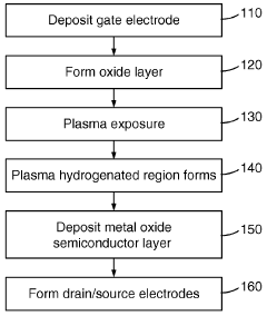
Innovation
- Exposing the dielectric layer to a hydrogen-containing plasma before depositing the metal oxide semiconductor layer creates a hydrogenated region at the semiconductor-dielectric interface, enhancing carrier mobility and reducing hysteresis, thereby stabilizing the TFTs.
Metal oxide thin film transistor with excellent temperature stability
PatentInactiveJP2016502278A
Innovation
- Implementing a passivation material with a conduction band at least 0.5 eV higher than the metal oxide semiconductor's conduction band to transfer electrons away from the interface, reducing oxygen loss and improving stability by selecting materials like Ta2O5, TiO2, or other insulating oxides that are less susceptible to reduction.
Space and Nuclear Applications Assessment
Metal oxide thin-film transistors (TFTs) have emerged as promising candidates for radiation-resistant electronics applications in both space and nuclear environments. These harsh operational settings expose electronic components to various forms of radiation, including gamma rays, neutrons, and high-energy particles, necessitating specialized materials and device architectures that can maintain functionality under such extreme conditions.
In space applications, metal oxide TFTs demonstrate significant advantages over conventional silicon-based technologies. Satellite systems, space probes, and orbital platforms require electronics that can withstand solar flares, cosmic rays, and trapped radiation belts. Studies have shown that amorphous indium-gallium-zinc-oxide (IGZO) TFTs exhibit remarkable radiation hardness, with minimal threshold voltage shifts even after exposure to total ionizing doses exceeding 1 Mrad(Si). This performance superiority stems from the unique electronic structure of metal oxides, where radiation-induced defects have limited impact on carrier transport mechanisms.
Nuclear applications present even more demanding radiation environments. In nuclear power plants, waste management facilities, and fusion research installations, electronics must function reliably while exposed to intense radiation fields. Recent experiments with hafnium-indium-zinc-oxide (HIZO) TFTs have demonstrated operational stability under neutron fluences up to 10^15 n/cm², outperforming conventional CMOS technologies by orders of magnitude. These results position metal oxide TFTs as viable solutions for instrumentation, control systems, and monitoring equipment in nuclear facilities.
The radiation resistance mechanisms of metal oxide TFTs derive from their fundamental material properties. The amorphous structure lacks grain boundaries that typically serve as defect accumulation sites in polycrystalline materials. Additionally, the predominant conduction mechanism involves spherically symmetric s-orbitals of metal cations, which are less susceptible to displacement damage than the directional sp³ bonds in silicon. These inherent advantages translate to extended operational lifetimes and reduced performance degradation in radiation-intensive environments.
Economic analyses indicate significant potential cost savings through the implementation of metal oxide TFT technologies in space and nuclear applications. The reduced need for radiation shielding, longer replacement intervals, and enhanced mission reliability contribute to favorable total ownership cost projections. Industry forecasts suggest a compound annual growth rate of 18% for radiation-hardened metal oxide electronics in these specialized sectors over the next decade.
Reliability Testing Methodologies and Standards
Reliability testing methodologies for Metal Oxide TFTs in radiation environments require specialized approaches that differ significantly from conventional semiconductor testing. The primary testing standards currently employed include MIL-STD-883 for microelectronic devices and JEDEC JESD57 for semiconductor device total ionizing dose testing, which have been adapted specifically for thin-film transistor technologies.
Total Ionizing Dose (TID) testing represents the cornerstone methodology for evaluating radiation hardness in metal oxide TFTs. This procedure typically involves exposing devices to gamma radiation from Co-60 sources at controlled dose rates ranging from 50 to 300 rad(Si)/s, with cumulative doses extending from 10 krad to 1 Mrad. Parameter extraction occurs at predetermined dose intervals to track threshold voltage shifts, mobility degradation, and subthreshold swing variations.
Single Event Effects (SEE) testing constitutes another critical evaluation protocol, utilizing heavy ion or proton beams to simulate cosmic radiation impacts. Testing facilities such as the Berkeley Laboratory Accelerator Space Effects (BLASE) and Texas A&M Cyclotron Institute provide standardized environments for these assessments. The linear energy transfer (LET) threshold determination serves as a key metric, typically ranging from 15-40 MeV·cm²/mg for radiation-hardened metal oxide TFT structures.
Temperature-dependent reliability testing forms an essential component of comprehensive evaluation protocols. Standard procedures involve bias temperature stress (BTS) testing at elevated temperatures (85°C to 150°C) under various gate bias conditions, both before and after radiation exposure. This methodology reveals the complex interplay between radiation-induced defects and temperature-activated charge trapping mechanisms in the gate dielectric and semiconductor interface.
Accelerated lifetime testing methodologies have been specifically modified for metal oxide TFTs to account for radiation effects. The Arrhenius model parameters require adjustment, as activation energies for defect formation and migration differ significantly between irradiated and non-irradiated devices. Typical acceleration factors range from 5x to 20x depending on the specific metal oxide composition and device architecture.
Statistical reliability assessment frameworks have evolved to address the unique variability challenges in radiation environments. Monte Carlo simulation approaches incorporating radiation damage models have been standardized to predict device parameter distributions after exposure. These methodologies typically require minimum sample sizes of 25-30 devices per test condition to establish statistical significance in parameter shift distributions.
Emerging standards specifically addressing metal oxide TFT radiation testing are currently under development through IEEE and JEDEC working groups, with draft specifications expected to be formalized within the next 18-24 months. These standards aim to establish unified test conditions, measurement protocols, and qualification criteria specifically tailored to the unique radiation response mechanisms observed in metal oxide semiconductor technologies.
Unlock deeper insights with Patsnap Eureka Quick Research — get a full tech report to explore trends and direct your research. Try now!
Generate Your Research Report Instantly with AI Agent
Supercharge your innovation with Patsnap Eureka AI Agent Platform!