Metal Oxide TFTs vs Graphene-Based TFTs: A Comparative Review
SEP 28, 20259 MIN READ
Generate Your Research Report Instantly with AI Agent
Patsnap Eureka helps you evaluate technical feasibility & market potential.
TFT Evolution and Research Objectives
Thin-Film Transistor (TFT) technology has undergone remarkable evolution since its inception in the 1960s. Initially developed as an alternative to silicon-based transistors, TFTs have transformed from simple switching elements to sophisticated components powering modern display technologies. The trajectory began with amorphous silicon (a-Si) TFTs, which dominated the market for decades despite limitations in electron mobility and stability.
The early 2000s witnessed a paradigm shift with the emergence of metal oxide semiconductors, particularly indium gallium zinc oxide (IGZO). These materials offered superior electron mobility, transparency, and lower power consumption compared to a-Si counterparts. This advancement enabled the development of high-resolution displays with enhanced performance characteristics, catalyzing the proliferation of smartphones and ultra-high-definition televisions.
Concurrently, carbon-based materials, especially graphene, emerged as potential game-changers in TFT technology. Discovered in 2004, graphene's exceptional electrical properties—including theoretical electron mobility exceeding 200,000 cm²/Vs—promised revolutionary improvements in TFT performance. However, the practical implementation of graphene-based TFTs has faced significant challenges, including the absence of an intrinsic bandgap and difficulties in large-scale manufacturing.
The current technological landscape presents a fascinating dichotomy: metal oxide TFTs have achieved commercial success and widespread adoption, while graphene-based alternatives remain predominantly in research laboratories despite their theoretical superiority. This divergence underscores the complex interplay between fundamental material properties and practical implementation considerations in semiconductor technology development.
Our research objectives focus on conducting a comprehensive comparative analysis of metal oxide and graphene-based TFTs across multiple dimensions. We aim to evaluate performance metrics including electron mobility, on/off current ratio, threshold voltage stability, and power efficiency. Additionally, we will assess manufacturing scalability, production costs, and environmental impact of both technologies.
Furthermore, this investigation seeks to identify potential hybrid approaches that might leverage the strengths of both material systems. By examining recent breakthroughs in doping techniques, contact engineering, and device architectures, we hope to outline pathways for overcoming current limitations. The ultimate goal is to provide strategic insights for future R&D investments and to forecast the evolution of TFT technology over the next decade, particularly for emerging applications in flexible electronics, transparent displays, and wearable computing devices.
Market Applications and Demand Analysis
The display industry has witnessed significant growth in demand for thin-film transistor (TFT) technologies, with the global TFT market projected to reach $127.5 billion by 2025. This growth is primarily driven by the expanding applications of TFTs in various sectors, particularly in consumer electronics, automotive displays, and emerging flexible electronics.
Metal oxide TFTs, especially those based on indium gallium zinc oxide (IGZO), have established a strong market presence in commercial display applications. These devices currently dominate the high-resolution display market, with major manufacturers like Sharp, LG, and Samsung incorporating them into premium television panels and smartphone displays. The market share of metal oxide TFTs in the display industry has grown steadily, capturing approximately 30% of the active-matrix display market.
The automotive sector represents a rapidly expanding application area for metal oxide TFTs, with increasing integration in dashboard displays, infotainment systems, and heads-up displays. This growth is attributed to their superior performance in high-temperature environments and excellent optical transparency, making them ideal for automotive applications where reliability and visibility are paramount.
Graphene-based TFTs, while still emerging in commercial applications, are generating significant interest in specialized markets that require exceptional flexibility, transparency, and electrical performance. The wearable technology sector has shown particular enthusiasm for graphene TFTs, with market research indicating a potential compound annual growth rate of 25% for graphene-based flexible display components over the next five years.
Healthcare applications represent another promising market for graphene TFTs, particularly in biosensors and medical monitoring devices. The biocompatibility and sensitivity of graphene make these transistors excellent candidates for next-generation medical devices, with several startups securing substantial funding to develop graphene-based healthcare monitoring systems.
The industrial and military sectors are also exploring specialized applications for both technologies. Metal oxide TFTs are finding applications in industrial control systems operating in harsh environments, while graphene TFTs are being evaluated for military applications requiring lightweight, flexible displays and sensors that can withstand extreme conditions.
Market analysis indicates that while metal oxide TFTs will continue to dominate the mass-market display industry in the near term, graphene-based TFTs are positioned to capture high-value niche markets where their unique properties offer significant advantages. The complementary nature of these technologies suggests that both will find sustainable market positions, with metal oxide TFTs serving mainstream applications and graphene TFTs addressing specialized needs requiring ultimate performance in flexibility, transparency, or sensing capabilities.
Current Challenges in TFT Technologies
Despite significant advancements in thin-film transistor (TFT) technologies, both metal oxide and graphene-based TFTs face substantial challenges that impede their widespread commercial adoption. Metal oxide TFTs, particularly those based on IGZO (Indium Gallium Zinc Oxide), struggle with stability issues under prolonged bias stress and environmental factors such as humidity and temperature fluctuations. The presence of oxygen vacancies in these materials, while beneficial for carrier transport, creates trap states that contribute to threshold voltage shifts during operation.
Manufacturing scalability presents another significant hurdle for metal oxide TFTs. While they offer better uniformity than amorphous silicon, achieving consistent performance across large-area substrates remains problematic. The deposition processes, typically sputtering or solution processing, require precise control of oxygen partial pressure and post-deposition annealing, which complicates integration with temperature-sensitive substrates for flexible electronics.
Graphene-based TFTs face their own set of distinct challenges. The absence of an intrinsic bandgap in pristine graphene results in poor on/off current ratios, typically below 10, which is inadequate for most switching applications. Various approaches to induce a bandgap, such as creating graphene nanoribbons or chemical functionalization, often compromise the material's exceptional carrier mobility, negating its primary advantage.
The contact resistance at metal-graphene interfaces represents another significant limitation for graphene TFTs. The work function mismatch between metals and graphene creates Schottky barriers that impede carrier injection, resulting in performance degradation. Additionally, the surface sensitivity of graphene makes device characteristics highly dependent on substrate interactions and environmental adsorbates, leading to reliability concerns in practical applications.
From a manufacturing perspective, producing high-quality, large-area graphene with consistent properties remains challenging. Current methods like chemical vapor deposition (CVD) produce graphene that requires transfer processes from growth substrates to device substrates, introducing contaminants and structural defects. Solution-processed graphene oxide reduction methods offer better scalability but yield materials with inferior electronic properties compared to pristine graphene.
Both technologies also face integration challenges with existing manufacturing infrastructure. Metal oxide TFTs require specialized deposition equipment and precise control of oxygen content, while graphene TFTs demand entirely new processing protocols that are not yet standardized in the display or integrated circuit industries. These manufacturing hurdles significantly impact production costs and hinder the transition from laboratory demonstrations to commercial products.
Metal Oxide vs Graphene TFT Solutions
01 Metal oxide semiconductor materials for TFTs
Metal oxide semiconductors, such as zinc oxide, indium gallium zinc oxide (IGZO), and other transparent conducting oxides, are used as channel materials in thin-film transistors. These materials offer advantages including high electron mobility, good transparency, and compatibility with low-temperature processing. Metal oxide TFTs can be fabricated on various substrates and show excellent stability and performance characteristics suitable for display applications.- Metal oxide semiconductor materials for TFTs: Metal oxide semiconductors, particularly those based on zinc, indium, gallium, and tin oxides, are used as channel materials in thin-film transistors. These materials offer advantages such as high electron mobility, good transparency, and compatibility with low-temperature processing. The composition and deposition methods of these metal oxides significantly influence the performance characteristics of the resulting TFTs, including threshold voltage, on/off ratio, and stability under bias stress conditions.
- Graphene-based materials for TFT applications: Graphene and its derivatives are utilized as channel materials in thin-film transistors due to their exceptional electrical properties, including high carrier mobility and conductivity. Various methods for synthesizing and integrating graphene into TFT structures have been developed, such as chemical vapor deposition, mechanical exfoliation, and solution processing. Modifications to graphene, including doping and functionalization, can be employed to tune its electronic properties for specific TFT applications.
- Hybrid and composite TFT structures: Hybrid structures combining metal oxides with graphene or other materials create TFTs with enhanced performance characteristics. These composite approaches can leverage the advantages of multiple materials, such as the high mobility of graphene with the good on/off ratio of metal oxides. Various integration strategies include layered structures, nanocomposites, and heterojunctions that optimize electrical performance while maintaining compatibility with existing fabrication processes.
- Fabrication techniques and process optimization: Advanced fabrication methods for both metal oxide and graphene-based TFTs include solution processing, atomic layer deposition, sputtering, and various printing techniques. Low-temperature processing enables compatibility with flexible substrates, while patterning techniques such as photolithography and etching are optimized for high-resolution device structures. Post-deposition treatments including annealing and surface modifications are employed to enhance device performance and stability.
- Applications and device integration: Metal oxide and graphene-based TFTs are integrated into various electronic applications including display technologies, sensors, memory devices, and flexible electronics. Circuit design considerations address the specific characteristics of these materials, while integration with other components creates functional systems. The unique properties of these TFTs enable novel applications such as transparent electronics, wearable devices, and large-area electronics that benefit from their combination of electrical performance and physical attributes.
02 Graphene-based channel materials for TFTs
Graphene, a two-dimensional carbon material, is utilized as a channel material in thin-film transistors due to its exceptional electrical properties, including high carrier mobility and conductivity. Graphene-based TFTs can be fabricated through various methods including chemical vapor deposition (CVD) and reduction of graphene oxide. These transistors exhibit unique characteristics such as ambipolar transport behavior and mechanical flexibility, making them suitable for flexible electronics applications.Expand Specific Solutions03 Fabrication methods and device structures
Various fabrication techniques are employed for both metal oxide and graphene-based TFTs, including solution processing, vacuum deposition, and transfer methods. Device structures can be configured as bottom-gate, top-gate, or dual-gate architectures with different electrode materials and dielectric layers. Advanced fabrication methods focus on improving interface quality, reducing contact resistance, and enabling low-temperature processing for compatibility with flexible substrates.Expand Specific Solutions04 Performance enhancement techniques
Various approaches are used to enhance the performance of both metal oxide and graphene-based TFTs. These include surface treatment and passivation techniques, doping strategies, interface engineering, and hybrid material integration. Additional methods involve optimizing the dielectric layer, controlling oxygen vacancies in metal oxides, and modifying the graphene structure through functionalization or patterning to improve mobility, on/off ratio, threshold voltage stability, and other key performance parameters.Expand Specific Solutions05 Applications in electronic devices
Metal oxide and graphene-based TFTs are implemented in various electronic applications including display technologies (such as OLED displays and LCD panels), flexible electronics, transparent circuits, sensors, and memory devices. The unique properties of these materials enable the development of next-generation devices with improved performance characteristics including higher refresh rates, better power efficiency, transparency, and mechanical flexibility. Integration strategies with conventional electronics and specialized circuit designs are developed to maximize the advantages of these novel TFT technologies.Expand Specific Solutions
Leading Manufacturers and Research Institutions
The metal oxide TFT and graphene-based TFT market is currently in a transitional phase, with metal oxide technology reaching commercial maturity while graphene remains largely in research and development. The global TFT market is projected to exceed $120 billion by 2025, with metal oxide TFTs dominating commercial applications. Companies like BOE Technology, LG Display, and Sharp have established mass production capabilities for metal oxide TFTs, particularly IGZO technology. Meanwhile, research institutions like Peking University Shenzhen Graduate School and Imec are advancing graphene-based TFTs, with Applied Materials and Semiconductor Energy Laboratory developing manufacturing processes. The competitive landscape shows established display manufacturers investing in metal oxide technology while collaborating with research organizations to explore graphene's potential for next-generation flexible and transparent electronics.
BOE Technology Group Co., Ltd.
Technical Solution: BOE has implemented advanced metal oxide TFT technology across multiple display product lines, focusing primarily on IGZO (Indium Gallium Zinc Oxide) backplanes for both LCD and OLED applications. Their oxide TFT technology achieves electron mobility of 10-15 cm²/Vs with excellent uniformity across Gen 10.5 substrates (2940×3370mm). BOE's proprietary compensation circuits and gate driver integration techniques have enabled oxide TFT displays with refresh rates exceeding 240Hz while maintaining power efficiency. For flexible display applications, BOE has developed low-temperature oxide TFT processes compatible with plastic substrates, achieving bend radii below 5mm without performance degradation. In parallel, BOE's research division has explored graphene-based TFTs, demonstrating laboratory prototypes with carrier mobility exceeding 200 cm²/Vs and optical transparency above 90%. Their comparative analysis indicates that while graphene offers theoretical advantages in mobility and flexibility, current manufacturing challenges including contact resistance issues and channel uniformity limitations have kept oxide TFTs as their primary commercial technology.
Strengths: Massive production capacity for oxide TFT displays; vertical integration from materials to finished products; established supply chain and manufacturing expertise; proven reliability in commercial products. Weaknesses: Higher power consumption compared to theoretical graphene TFT performance; limited flexibility compared to potential graphene solutions; relatively higher operating voltages required for equivalent performance.
Applied Materials, Inc.
Technical Solution: Applied Materials has developed comprehensive manufacturing solutions for both metal oxide and graphene-based TFT production. Their AKT PECVD systems enable large-area deposition of high-quality oxide semiconductors with thickness uniformity below ±5% across Gen 10.5 substrates. For metal oxide TFTs, Applied Materials' integrated PVD-based approach delivers IGZO films with carrier mobility consistently above 15 cm²/Vs and stability under bias stress conditions with threshold voltage shifts below 1V after 10,000 seconds of constant bias. Their proprietary Etch and CVD technologies support self-aligned TFT structures that minimize parasitic capacitance, enabling faster switching speeds essential for high refresh rate displays. For graphene-based TFTs, Applied Materials has pioneered roll-to-roll CVD processes capable of synthesizing graphene films with sheet resistance below 300 Ω/sq and mobility exceeding 500 cm²/Vs. Their comparative analysis demonstrates that while graphene TFTs offer superior theoretical performance, oxide TFTs currently provide better manufacturing yield and cost-effectiveness for commercial display applications.
Strengths: Comprehensive equipment portfolio supporting both technologies; deep expertise in scaling manufacturing processes; ability to provide end-to-end solutions from material deposition to device integration. Weaknesses: Equipment-focused approach rather than direct device manufacturing; reliance on display manufacturers to implement and optimize processes; higher initial capital investment requirements for graphene TFT production lines.
Key Patents and Scientific Breakthroughs
Thin-film transistor
PatentWO2020247640A1
Innovation
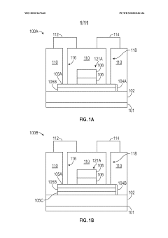
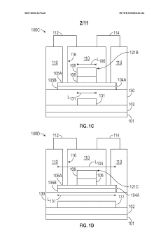
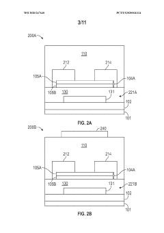
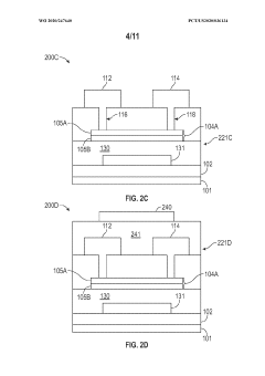
- The implementation of multi-layer semiconductor channel stacks with alternating electron mobilities, combining low and high mobility layers to enhance carrier density and reduce off-leakage current, resulting in improved TFT performance with higher on current and positive threshold voltage.
Thin film transistor
PatentActiveUS20150069379A1
Innovation
- A thin film transistor with an indium gallium zinc oxide (IGZO) semiconductor layer, where the atomic ratios of gallium to indium and zinc are optimized between 1.5 to 2, enhancing the stability and reliability by maintaining mobility greater than 10 cm2/Vs and reducing threshold voltage variation to less than 1.3 V, and subthreshold swing to less than 0.6 V/dec.
Manufacturing Process Comparison
The manufacturing processes for Metal Oxide TFTs and Graphene-Based TFTs represent distinct technological approaches with significant implications for performance, cost, and scalability. Metal oxide TFTs, particularly those based on amorphous Indium Gallium Zinc Oxide (a-IGZO), have achieved commercial success due to their relatively mature manufacturing processes. These devices typically employ physical vapor deposition (PVD) techniques such as sputtering, which can be performed at relatively low temperatures (200-300°C) and are compatible with existing display manufacturing infrastructure.
The industrial-scale production of metal oxide TFTs benefits from established photolithography processes and can achieve high throughput on large-area substrates. This manufacturing maturity translates to lower production costs and higher yield rates compared to emerging alternatives. Additionally, the stability of metal oxide precursors and their compatibility with standard clean room environments further enhances their manufacturability.
In contrast, graphene-based TFTs present more complex manufacturing challenges despite their promising electrical properties. The production of high-quality graphene films remains a significant hurdle for mass production. Current methods include chemical vapor deposition (CVD), which can produce large-area graphene but often introduces defects that compromise device performance. Alternative approaches such as epitaxial growth on SiC substrates yield higher quality material but at substantially higher costs.
Transfer processes represent another critical manufacturing challenge for graphene TFTs. After growth, graphene typically requires transfer from its growth substrate to the target substrate, introducing potential contamination and structural defects. This transfer step significantly impacts yield rates and device uniformity, creating bottlenecks in scaling production.
Recent advancements in solution-processed graphene offer promising alternatives for large-scale manufacturing. Techniques involving graphene oxide reduction or liquid-phase exfoliation can be compatible with printing technologies, potentially enabling roll-to-roll processing. However, these methods currently produce graphene with higher defect densities and lower carrier mobilities compared to CVD-grown material.
The integration of contacts and dielectric layers presents different challenges for each technology. Metal oxide TFTs benefit from established processes for depositing and patterning these layers, while graphene TFTs require careful interface engineering to preserve graphene's intrinsic properties. The high sensitivity of graphene to processing conditions necessitates specialized approaches to prevent performance degradation during manufacturing.
From a sustainability perspective, metal oxide TFTs face concerns regarding indium scarcity and potential environmental impact, while graphene production currently involves energy-intensive processes and potentially hazardous chemicals. As manufacturing technologies evolve, addressing these sustainability challenges will become increasingly important for both technologies.
Sustainability and Environmental Impact
The sustainability and environmental impact of thin-film transistor (TFT) technologies have become increasingly important considerations in the electronics industry. Metal oxide TFTs and graphene-based TFTs present distinct environmental profiles throughout their lifecycle, from raw material extraction to end-of-life disposal.
Metal oxide TFTs typically utilize materials such as indium, gallium, zinc, and tin. The extraction of these elements, particularly indium, raises significant sustainability concerns due to its limited natural abundance and energy-intensive mining processes. However, metal oxide TFTs benefit from established manufacturing infrastructure that has been optimized for efficiency over decades, potentially reducing their overall carbon footprint during production.
Graphene-based TFTs, conversely, rely primarily on carbon, one of the most abundant elements on Earth. The raw material acquisition for graphene can be considerably more sustainable, especially when derived from renewable carbon sources. Production methods such as chemical vapor deposition (CVD) and liquid-phase exfoliation vary significantly in their environmental impact, with some processes requiring high temperatures and hazardous chemicals while others employ more environmentally benign approaches.
Energy consumption during device operation represents another critical environmental factor. Metal oxide TFTs typically require higher operating voltages compared to their graphene counterparts, resulting in greater power consumption over the device lifetime. Graphene-based TFTs demonstrate superior electron mobility, enabling lower voltage operation and potentially reducing the energy demands of electronic devices incorporating this technology.
Durability and lifespan also factor into the sustainability equation. Metal oxide TFTs have demonstrated excellent stability under various environmental conditions, potentially extending device lifespans and reducing electronic waste. Graphene-based TFTs show promising mechanical flexibility but may face challenges regarding long-term stability in certain applications, which could impact their overall environmental footprint through shortened replacement cycles.
End-of-life considerations reveal further distinctions. The recovery and recycling of rare metals from metal oxide TFTs present both an environmental necessity and a technical challenge. Graphene-based devices may offer simpler recycling pathways due to their carbon-based composition, though the presence of substrate materials and other components can complicate recovery efforts.
Emerging research in green manufacturing techniques for both technologies shows promise for reducing environmental impacts. Innovations such as solution-processing methods for metal oxides and environmentally friendly graphene production techniques could significantly improve the sustainability profiles of both TFT types in the coming years, potentially narrowing the gap between their respective environmental footprints.
Unlock deeper insights with Patsnap Eureka Quick Research — get a full tech report to explore trends and direct your research. Try now!
Generate Your Research Report Instantly with AI Agent
Supercharge your innovation with Patsnap Eureka AI Agent Platform!
