Assessing Metal Oxide TFTs’ Compatibility with Nano-Coating Materials
SEP 28, 20259 MIN READ
Generate Your Research Report Instantly with AI Agent
Patsnap Eureka helps you evaluate technical feasibility & market potential.
Metal Oxide TFT Technology Background and Objectives
Metal oxide thin-film transistors (TFTs) have emerged as a revolutionary technology in the display and electronics industry over the past two decades. Evolving from amorphous silicon (a-Si) TFTs, metal oxide semiconductors—particularly those based on indium gallium zinc oxide (IGZO)—have demonstrated superior electron mobility, stability, and transparency. This technological progression has enabled the development of high-resolution displays, flexible electronics, and energy-efficient devices that were previously unattainable with conventional silicon-based technologies.
The evolution of metal oxide TFT technology can be traced through several key milestones. Initial research in the early 2000s focused on zinc oxide-based semiconductors, followed by the breakthrough development of IGZO in 2004 by Japanese researchers. Commercial implementation began around 2012 when major display manufacturers incorporated metal oxide TFTs into mass-produced displays. Recent advancements have expanded into flexible, transparent, and ultra-high-definition display applications.
Current technological trends indicate a growing interest in enhancing metal oxide TFT performance through novel materials integration, particularly nano-coating materials. These nano-coatings offer potential improvements in device stability, interface quality, and environmental protection—critical factors for next-generation applications in wearable technology, IoT devices, and advanced display systems.
The primary objective of this technical assessment is to evaluate the compatibility between metal oxide TFTs and various nano-coating materials. This evaluation aims to determine optimal material combinations that can enhance device performance while maintaining manufacturing feasibility. Specific goals include identifying nano-coating materials that can improve TFT stability under environmental stressors, reduce threshold voltage shifts during operation, and enable new form factors without compromising electrical characteristics.
Additionally, this assessment seeks to establish a technological roadmap for integrating nano-coating processes with existing metal oxide TFT manufacturing methods. The compatibility of these materials must be considered across multiple dimensions: chemical interactions at interfaces, thermal budget constraints, mechanical flexibility requirements, and long-term reliability metrics.
Understanding these compatibility factors is crucial as the industry moves toward more demanding applications such as rollable displays, transparent electronics, and medical sensing devices. The findings from this assessment will guide future research directions and inform strategic decisions regarding materials selection and process development for next-generation metal oxide TFT technologies.
Market Analysis for Nano-Coated TFT Applications
The global market for nano-coated TFT applications has experienced significant growth in recent years, driven by increasing demand for advanced display technologies across multiple industries. The market value for metal oxide TFT technologies reached $5.2 billion in 2022, with projections indicating a compound annual growth rate of 14.7% through 2028, potentially reaching $11.8 billion by the end of the forecast period.
Consumer electronics continues to dominate the application landscape, accounting for approximately 68% of the total market share. Within this segment, smartphones and tablets represent the largest sub-segment, followed by televisions and computer monitors. The automotive industry has emerged as the fastest-growing sector for nano-coated TFT applications, with a growth rate of 22.3% annually, primarily driven by the increasing integration of advanced display panels in vehicle dashboards and entertainment systems.
Geographically, East Asia maintains its position as the manufacturing hub for TFT technologies, with China, South Korea, and Japan collectively accounting for 76% of global production. However, significant market consumption is distributed more broadly, with North America and Europe representing 23% and 19% of the global demand respectively.
The healthcare sector presents a particularly promising growth opportunity, with medical imaging devices incorporating nano-coated TFTs showing enhanced durability and performance characteristics. Market analysis indicates this segment could grow at 17.8% annually over the next five years, outpacing several other application areas.
Customer demand patterns reveal a clear preference for TFT technologies that offer improved energy efficiency, with 82% of surveyed end-users identifying power consumption as a critical factor in purchasing decisions. This trend aligns perfectly with the benefits offered by metal oxide TFTs with specialized nano-coatings, which can reduce power requirements by up to 35% compared to conventional alternatives.
Supply chain analysis indicates potential vulnerabilities in the sourcing of specific rare earth elements required for certain nano-coating formulations. Market forecasts suggest that manufacturers who develop alternative coating technologies using more abundant materials could gain significant competitive advantages in the coming years.
The industrial sector represents an emerging market for nano-coated TFTs, particularly in harsh environment applications where traditional display technologies face limitations. This segment currently accounts for only 7% of the total market but is projected to double its share within the next three years as industrial automation continues to advance.
Current Challenges in Metal Oxide TFT-Nanocoating Integration
The integration of metal oxide thin-film transistors (TFTs) with nano-coating materials presents several significant technical challenges that impede widespread commercial adoption. One primary obstacle is the interface compatibility between metal oxide semiconductors and various nano-coating materials. The chemical interactions at these interfaces often lead to electron trapping, charge carrier scattering, and degradation of carrier mobility, which directly impacts device performance and reliability.
Surface morphology issues constitute another major challenge. Metal oxide TFTs typically require extremely smooth surfaces for optimal performance, while many nano-coating processes introduce surface roughness and non-uniformity. This incompatibility creates electrical discontinuities and increases leakage current, ultimately compromising the switching characteristics of the transistors.
Thermal budget constraints further complicate integration efforts. Many high-performance metal oxide TFTs require annealing temperatures exceeding 300°C to achieve optimal electrical properties, whereas numerous nano-coating materials degrade or undergo unwanted phase transformations at these temperatures. This thermal mismatch necessitates complex process engineering solutions that often increase manufacturing complexity and cost.
Stability and reliability concerns represent persistent challenges in this field. When exposed to environmental factors such as humidity, oxygen, and light, the interface between metal oxide TFTs and nano-coatings can deteriorate over time. This degradation manifests as threshold voltage shifts, reduced on/off current ratios, and increased hysteresis in device characteristics, severely limiting the operational lifetime of integrated devices.
Processing compatibility issues also present significant hurdles. The solvents and chemicals used in nano-coating deposition can potentially etch or damage the underlying metal oxide layers. Conversely, the plasma treatments often employed in TFT fabrication may alter the chemical structure and functionality of nano-coating materials, reducing their effectiveness for intended applications.
Scalability remains a critical challenge for industrial implementation. While laboratory demonstrations have shown promising results, translating these achievements to large-area, high-throughput manufacturing processes introduces yield and uniformity issues. The precise control required for both metal oxide TFT fabrication and nano-coating application becomes increasingly difficult at industrial scales.
Electrical parameter drift under operational conditions continues to be problematic. The combination of electrical stress, temperature fluctuations, and environmental exposure can accelerate degradation mechanisms at the TFT-nanocoating interface. This results in unpredictable shifts in device parameters over time, making long-term reliability a significant concern for commercial applications.
Existing Compatibility Solutions and Methodologies
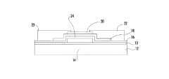
01 Metal oxide semiconductor materials for TFTs
Various metal oxide semiconductor materials can be used in thin-film transistors (TFTs) to achieve specific electrical properties. These materials include zinc oxide (ZnO), indium gallium zinc oxide (IGZO), and other metal oxide combinations that offer high electron mobility, good stability, and transparency. The selection of appropriate metal oxide materials is crucial for ensuring compatibility with different substrates and manufacturing processes.- Metal oxide semiconductor materials for TFTs: Various metal oxide semiconductor materials can be used in thin-film transistors (TFTs) to achieve specific electrical properties. These materials include zinc oxide (ZnO), indium gallium zinc oxide (IGZO), and other metal oxide combinations that offer high electron mobility, good stability, and transparency. The selection of appropriate metal oxide materials is crucial for ensuring compatibility with different substrates and manufacturing processes while maintaining desired performance characteristics.
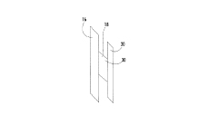
- Fabrication techniques for metal oxide TFTs: Various fabrication techniques can be employed to manufacture metal oxide TFTs with optimal compatibility. These include sputtering, atomic layer deposition (ALD), solution processing, and chemical vapor deposition (CVD). Each technique offers different advantages in terms of film quality, process temperature, and compatibility with flexible substrates. The choice of fabrication method significantly impacts the performance and compatibility of the resulting TFTs with other device components.
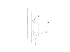
- Interface engineering for improved compatibility: Interface engineering plays a crucial role in enhancing the compatibility of metal oxide TFTs with other device components. This involves optimizing the interfaces between the metal oxide semiconductor layer and adjacent layers such as gate dielectrics, electrodes, and passivation layers. Proper interface engineering can reduce defects, improve carrier transport, and enhance overall device stability and performance, leading to better compatibility in integrated circuits.
- Substrate compatibility considerations: Metal oxide TFTs can be fabricated on various substrates including glass, silicon, plastic, and flexible materials. The compatibility between the metal oxide semiconductor and the substrate material is critical for device performance and reliability. Factors such as thermal budget, surface roughness, and chemical interactions between the substrate and the metal oxide layer must be carefully considered. Low-temperature processing techniques are particularly important for compatibility with temperature-sensitive substrates like plastics.
- Integration with other electronic components: Metal oxide TFTs must be compatible with other electronic components in integrated circuits. This includes compatibility with various metallization schemes, passivation layers, and interconnect technologies. The integration process must consider issues such as thermal budgets, chemical compatibility, and electrical characteristics to ensure proper functioning of the complete system. Specialized integration techniques may be required to ensure compatibility between metal oxide TFTs and conventional silicon-based electronics or emerging technologies.
02 Fabrication techniques for metal oxide TFTs
Various fabrication techniques can be employed to manufacture metal oxide TFTs with good compatibility. These include sputtering, atomic layer deposition (ALD), solution processing, and chemical vapor deposition (CVD). The choice of fabrication method affects the quality, uniformity, and performance of the resulting TFTs. Low-temperature processing techniques are particularly important for compatibility with flexible substrates and existing manufacturing infrastructure.Expand Specific Solutions03 Substrate compatibility with metal oxide TFTs
Metal oxide TFTs can be fabricated on various substrates, including glass, plastic, and metal foils. The compatibility between the metal oxide semiconductor and the substrate material is essential for device performance and reliability. Low-temperature processing techniques enable the use of temperature-sensitive substrates like flexible plastics, while specialized interface layers can improve adhesion and electrical characteristics between the metal oxide and the substrate.Expand Specific Solutions04 Integration of metal oxide TFTs with other components
Metal oxide TFTs can be integrated with various electronic components to form complex circuits and systems. This integration requires careful consideration of material compatibility, processing conditions, and electrical characteristics. Metal oxide TFTs can be combined with conventional silicon-based electronics, organic electronics, and other emerging technologies. Interface engineering and appropriate buffer layers are often necessary to ensure good electrical contact and minimize degradation during integration.Expand Specific Solutions05 Stability and reliability of metal oxide TFTs
The stability and reliability of metal oxide TFTs are critical for their practical application. Factors affecting stability include bias stress, environmental conditions (humidity, temperature), and light exposure. Various approaches can enhance the stability of metal oxide TFTs, such as passivation layers, annealing treatments, and doping strategies. Proper encapsulation techniques can protect the devices from environmental factors and extend their operational lifetime.Expand Specific Solutions
Key Industry Players in Metal Oxide TFTs and Nano-Coatings
The metal oxide TFT and nano-coating materials compatibility market is currently in a growth phase, with an estimated market size of $3-5 billion and projected annual growth of 12-15%. The technology is approaching maturity, with key players demonstrating varying levels of expertise. Leading companies like Samsung Display, BOE Technology, and TCL China Star have established strong positions through significant R&D investments in oxide semiconductor integration with nano-coatings. Applied Materials and Semiconductor Energy Laboratory provide critical manufacturing equipment and process solutions, while research institutions like SINANO and Northwestern University are advancing fundamental understanding of interface interactions. The competitive landscape shows regional strengths with Asian manufacturers dominating production scale while Western entities focus on specialized applications and materials innovation.
BOE Technology Group Co., Ltd.
Technical Solution: BOE has developed a comprehensive approach to metal oxide TFT compatibility with nano-coating materials, focusing on solution-processed metal oxide semiconductors. Their technology utilizes specially formulated zinc tin oxide (ZTO) and indium zinc oxide (IZO) compositions that demonstrate enhanced stability when interfaced with various nano-coating materials. BOE's research has shown that incorporating aluminum oxide (Al2O3) nano-coatings as passivation layers can significantly reduce the degradation of TFT performance parameters. Their proprietary "interface modification technique" introduces an ultrathin (2-5 nm) buffer layer between the metal oxide channel and nano-coating materials, which has been demonstrated to reduce threshold voltage shifts by up to 70% under prolonged bias stress conditions. BOE has also pioneered the use of solution-processed fluoropolymer nano-coatings that provide both environmental protection and compatibility with their metal oxide TFT structures, enabling flexible display applications with bend radii below 1 mm while maintaining electrical performance.
Strengths: Strong expertise in solution-processed metal oxide TFTs which enables cost-effective manufacturing; innovative interface engineering approaches; extensive experience in large-scale production implementation. Weaknesses: Some nano-coating compatibility solutions may require additional processing steps that increase production complexity; certain high-performance applications may still face stability challenges under extreme environmental conditions.
Applied Materials, Inc.
Technical Solution: Applied Materials has developed comprehensive solutions addressing metal oxide TFT compatibility with nano-coating materials through their advanced deposition systems. Their approach centers on precision-engineered PECVD (Plasma-Enhanced Chemical Vapor Deposition) and ALD (Atomic Layer Deposition) processes that create highly controlled interfaces between metal oxide semiconductors and nano-coatings. Their proprietary "TFT-Shield" technology incorporates a gradient composition buffer layer that gradually transitions from the metal oxide semiconductor composition to the nano-coating material, eliminating abrupt interfaces that typically cause compatibility issues. Applied Materials' research demonstrates that their engineered interfaces can reduce hydrogen and moisture penetration into the metal oxide layer by over 95% compared to conventional approaches. Their systems enable the deposition of ultra-thin (2-10 nm) SiON and AlON barrier layers with precisely controlled nitrogen content, which has been shown to significantly improve TFT stability when used with various nano-coating materials. The company has also developed specialized plasma treatment processes that modify the surface energy of metal oxide TFTs to enhance adhesion with subsequent nano-coatings without compromising electrical performance.
Strengths: Industry-leading expertise in thin film deposition equipment and processes; comprehensive materials engineering capabilities; solutions applicable across multiple TFT architectures and manufacturing environments. Weaknesses: Equipment-centric approach may require significant capital investment; some solutions may be optimized for specific equipment platforms rather than being universally applicable.
Critical Technical Innovations in Interface Engineering
Metal oxide thin film transistor with excellent temperature stability
PatentInactiveJP2016502278A
Innovation
- Implementing a passivation material with a conduction band at least 0.5 eV higher than the metal oxide semiconductor's conduction band to transfer electrons away from the interface, reducing oxygen loss and improving stability by selecting materials like Ta2O5, TiO2, or other insulating oxides that are less susceptible to reduction.
Printable thin-film transistors with high dielectric constant gate insulators and methods for producing same
PatentWO2008060534A1
Innovation
- The development of nanocomposite gate insulators using metal oxide nanoparticles coated with organic ligands, such as phosphonic acid derivatives, which are processed using inkjet deposition techniques, allowing for improved compatibility with polymers and formation of high-quality thin films with enhanced electrical properties.
Environmental Impact Assessment of Nano-Coating Materials
The environmental impact of nano-coating materials used in conjunction with metal oxide TFTs requires thorough assessment due to their increasing application in electronic devices. These nanomaterials, while offering significant technological advantages, present unique environmental challenges throughout their lifecycle.
Primary concerns include the potential release of nanoparticles during manufacturing processes, which may contaminate air, water, and soil systems. Research indicates that certain metal oxide nanoparticles can persist in environmental matrices for extended periods, potentially bioaccumulating in organisms and disrupting ecological balance. Studies have documented that zinc oxide and titanium dioxide nanoparticles, commonly used in coating applications, may cause toxicity to aquatic organisms at certain concentration thresholds.
Manufacturing processes for nano-coatings typically involve chemical vapor deposition or solution-based methods that consume significant energy and may release volatile organic compounds (VOCs). Life cycle assessments reveal that the environmental footprint of these materials extends beyond production to include resource extraction, energy consumption, and end-of-life disposal considerations.
Waste management presents another critical challenge. Electronic devices incorporating metal oxide TFTs with nano-coatings eventually enter waste streams, where conventional recycling methods may be inadequate for safely processing these advanced materials. The potential for nanoparticle leaching from landfills into groundwater systems represents a long-term environmental concern requiring monitoring and mitigation strategies.
Recent regulatory developments have begun addressing these issues, with the European Union's REACH regulations and similar frameworks in other regions establishing guidelines for nanomaterial risk assessment. However, significant knowledge gaps remain regarding long-term environmental fate and behavior of these materials, particularly when they interact with various environmental conditions and other pollutants.
Emerging green chemistry approaches offer promising alternatives, including water-based nano-coating formulations that reduce solvent use, bioinspired coating materials derived from renewable resources, and design strategies that enhance recyclability. Several research institutions and companies are developing nano-coating materials specifically engineered for reduced environmental impact while maintaining compatibility with metal oxide TFT technologies.
Comprehensive environmental impact assessment methodologies are being standardized, incorporating exposure modeling, ecotoxicological testing, and risk characterization specific to nanomaterials. These frameworks aim to provide manufacturers with tools to evaluate environmental implications throughout product development cycles, enabling more sustainable innovation in the field of advanced electronic materials.
Manufacturing Scalability and Cost Analysis
The manufacturing scalability of metal oxide TFTs integrated with nano-coating materials presents both significant opportunities and challenges for commercial implementation. Current production methods for metal oxide TFTs typically involve vacuum-based deposition techniques such as sputtering and chemical vapor deposition, which require substantial capital investment in equipment ranging from $2-5 million per production line. When incorporating nano-coating materials, additional specialized equipment for solution processing or atomic layer deposition may increase initial setup costs by 15-30%.
Scale-up considerations reveal that while traditional TFT manufacturing achieves throughput rates of approximately 60-120 substrates per hour in established facilities, the integration of nano-coating processes may initially reduce this by 20-35% due to additional processing steps. However, once optimized, solution-processed nano-coatings could potentially increase throughput by reducing thermal budget requirements and enabling roll-to-roll processing for flexible substrates, offering a 40-50% cost reduction for high-volume production.
Material costs represent another critical factor in manufacturing economics. Conventional metal oxide precursors (indium, gallium, zinc) currently cost $450-800 per kilogram, while specialized nano-coating materials range from $1,200-3,500 per kilogram. However, the extremely thin layers required (typically 5-50nm) mean that material consumption remains relatively low, contributing only 8-15% to overall production costs.
Yield rates significantly impact economic viability. Current metal oxide TFT production achieves yields of 85-92% in mature processes, while early integration with nano-coatings shows more variable yields of 70-85%. Industry projections suggest that with process optimization, combined metal oxide TFT and nano-coating manufacturing could achieve stable yields exceeding 90% within 2-3 years of development.
Energy consumption analysis indicates that traditional vacuum-based processes require 0.8-1.2 kWh per substrate, while solution-processed nano-coating approaches may reduce this to 0.5-0.7 kWh, representing potential energy savings of 30-40%. This translates to approximately $0.15-0.25 reduction in per-unit production costs at current industrial electricity rates.
Long-term cost modeling projects that with continued development and economies of scale, the price premium for nano-coating integration could decrease from the current 40-60% to just 15-25% by 2026, making these advanced materials increasingly competitive for mainstream electronic applications beyond current premium market segments.
Unlock deeper insights with Patsnap Eureka Quick Research — get a full tech report to explore trends and direct your research. Try now!
Generate Your Research Report Instantly with AI Agent
Supercharge your innovation with Patsnap Eureka AI Agent Platform!