Reviewing Metal Oxide TFTs’ Impact on Energy Harvesting Systems
SEP 28, 20259 MIN READ
Generate Your Research Report Instantly with AI Agent
Patsnap Eureka helps you evaluate technical feasibility & market potential.
Metal Oxide TFT Development History and Objectives
Metal oxide thin-film transistors (TFTs) emerged in the early 1990s when researchers began exploring transparent conducting oxides as semiconductor materials. The initial breakthrough came in 1996 with the development of zinc oxide (ZnO) based TFTs, which demonstrated promising electrical characteristics. However, these early devices suffered from stability issues and inconsistent performance, limiting their practical applications.
A significant advancement occurred in 2003 when researchers at the Tokyo Institute of Technology developed indium gallium zinc oxide (IGZO) TFTs, which exhibited substantially improved electron mobility and stability compared to their predecessors. This innovation marked a turning point in metal oxide TFT technology, enabling their consideration for commercial applications beyond laboratory settings.
The period between 2005 and 2010 witnessed rapid progress in fabrication techniques, with the introduction of room-temperature processing methods that dramatically reduced manufacturing costs. This development was crucial for expanding the potential application scope of metal oxide TFTs, particularly in flexible and large-area electronics where traditional silicon-based technologies faced limitations.
By 2012, major display manufacturers began incorporating metal oxide TFTs into commercial products, primarily in high-resolution displays. The superior electron mobility of these devices, compared to amorphous silicon alternatives, enabled faster switching speeds and lower power consumption, establishing their commercial viability.
The evolution of metal oxide TFTs has been driven by several key objectives. Foremost among these is achieving ultra-low power operation, essential for integration into energy harvesting systems where power availability is inherently limited. Researchers have focused on reducing threshold voltages and minimizing leakage currents to enable operation at sub-volt levels.
Another critical objective has been enhancing operational stability under various environmental conditions. Early metal oxide TFTs exhibited significant performance degradation when exposed to light, humidity, or temperature variations—a serious limitation for energy harvesting applications often deployed in challenging environments.
Mechanical flexibility represents another important development goal, particularly for integration with flexible energy harvesters such as piezoelectric or triboelectric generators. Recent research has focused on developing metal oxide TFTs on flexible substrates that can withstand repeated bending without performance deterioration.
The current technological trajectory aims to develop metal oxide TFTs capable of operating at extremely low power levels (<1 μW) while maintaining reliable performance characteristics. This would enable direct powering from ambient energy sources without requiring intermediate energy storage components, potentially revolutionizing self-powered electronic systems and autonomous sensor networks.
Energy Harvesting Market Demand Analysis
The energy harvesting market has experienced significant growth in recent years, driven by increasing demand for sustainable power solutions across multiple industries. Current market valuations place the global energy harvesting sector at approximately $600 million as of 2023, with projections indicating expansion to reach $1.3 billion by 2028, representing a compound annual growth rate (CAGR) of 16.7%. This growth trajectory reflects the escalating need for autonomous power solutions in applications ranging from consumer electronics to industrial IoT deployments.
Metal oxide thin-film transistors (TFTs) are positioned at a critical intersection within this expanding market, particularly as enabling components for more efficient energy harvesting systems. Market research indicates that approximately 35% of energy harvesting applications now require advanced semiconductor technologies like metal oxide TFTs to optimize power management and conversion efficiencies.
The industrial sector currently represents the largest market segment for energy harvesting technologies incorporating metal oxide TFTs, accounting for 42% of total market demand. This is primarily driven by the proliferation of wireless sensor networks in manufacturing environments, where self-powered sensors can significantly reduce maintenance costs and improve operational efficiency. Market analysis reveals that companies implementing such solutions report operational cost reductions averaging 27% over three-year deployment periods.
Consumer electronics constitutes the fastest-growing segment, with a projected CAGR of 22.3% through 2028. The integration of metal oxide TFTs in energy harvesting circuits for wearable devices, smartphones, and portable electronics is enabling longer battery life and new functionality. Market surveys indicate that 68% of consumers consider energy efficiency and battery performance as "very important" factors in purchasing decisions for portable electronic devices.
Regional analysis shows Asia-Pacific leading market growth with 41% of global market share, followed by North America (28%) and Europe (23%). China and South Korea are particularly significant markets due to their robust electronics manufacturing ecosystems and government initiatives supporting green technology development.
Key market drivers include increasing deployment of IoT devices (projected to reach 75 billion connected devices by 2025), growing demand for battery-free wireless sensors, and stringent energy efficiency regulations across developed economies. The market for energy harvesting solutions specifically utilizing metal oxide TFT technology is expected to grow at 19.2% CAGR, outpacing the broader energy harvesting market.
Customer demand is increasingly focused on integrated solutions that combine multiple harvesting technologies with efficient power management circuits based on advanced semiconductor technologies like metal oxide TFTs, creating significant opportunities for cross-industry collaboration and technological innovation.
Current Metal Oxide TFT Technology Landscape
Metal oxide thin-film transistors (TFTs) have emerged as a transformative technology in the semiconductor industry over the past decade. The current landscape of metal oxide TFT technology is characterized by significant advancements in materials science, fabrication techniques, and integration capabilities that have expanded their application potential beyond traditional display technologies into energy harvesting systems.
Amorphous oxide semiconductors (AOS), particularly indium-gallium-zinc-oxide (IGZO), have become the dominant material system in commercial applications due to their superior electron mobility (10-50 cm²/Vs), excellent uniformity, and low processing temperatures. These characteristics enable high performance on flexible substrates, making them ideal for integration with energy harvesting components. Major display manufacturers including Sharp, LG, and Samsung have successfully commercialized IGZO-based products, demonstrating the industrial maturity of this technology.
Recent developments have focused on enhancing stability under environmental stressors such as light, temperature, and bias stress. Passivation layers, compositional optimization, and interface engineering have significantly improved device reliability, extending operational lifetimes to meet the demanding requirements of energy harvesting applications. The development of solution-processed metal oxide TFTs has also gained momentum, offering cost-effective manufacturing routes through printing techniques that align with the economic constraints of energy harvesting systems.
The scaling capabilities of metal oxide TFTs have advanced considerably, with current technologies achieving channel lengths below 5 μm in production environments and research demonstrations approaching sub-micron dimensions. This miniaturization enables higher integration densities and reduced power consumption, critical factors for energy-limited harvesting systems. Additionally, innovations in device architecture, including dual-gate, vertical, and self-aligned structures, have enhanced performance metrics while maintaining fabrication compatibility.
Power management capabilities have been significantly improved through threshold voltage engineering and mobility enhancement techniques. Modern metal oxide TFTs can operate efficiently at voltages below 5V, with research prototypes demonstrating functionality at sub-1V levels. This low-voltage operation is particularly valuable for interfacing with the typically low-voltage outputs of energy harvesting transducers such as photovoltaic cells and piezoelectric generators.
Integration with other semiconductor technologies has progressed substantially, with demonstrated hybrid systems incorporating metal oxide TFTs alongside silicon CMOS, organic electronics, and emerging 2D materials. These heterogeneous integration approaches enable optimized system architectures that leverage the unique advantages of each technology while mitigating their individual limitations, creating more efficient and capable energy harvesting systems.
Current Integration Solutions for Energy Harvesting Systems
01 Metal oxide semiconductor materials for TFT fabrication
Metal oxide semiconductors, particularly those based on zinc, indium, gallium, and tin oxides, have emerged as promising materials for thin-film transistors (TFTs). These materials offer advantages such as high electron mobility, good transparency, and compatibility with low-temperature processing. The composition and deposition methods of these metal oxides significantly impact the electrical performance and stability of the resulting TFTs, enabling their application in next-generation display technologies.- Metal oxide semiconductor materials for TFT fabrication: Metal oxide semiconductors, particularly those based on zinc, indium, gallium, and tin oxides, have emerged as promising materials for thin-film transistors (TFTs). These materials offer advantages such as high electron mobility, good transparency, and compatibility with low-temperature processing. The composition and deposition methods of these metal oxides significantly impact the electrical performance and stability of the resulting TFTs, making them suitable for next-generation display technologies.
- Performance enhancement techniques for metal oxide TFTs: Various techniques have been developed to enhance the performance of metal oxide TFTs, including channel engineering, interface optimization, and post-deposition treatments. These approaches aim to improve key parameters such as carrier mobility, threshold voltage stability, and on/off current ratio. Specific methods include annealing processes, surface passivation, and the incorporation of dopants to modify the electronic properties of the metal oxide semiconductor layer, resulting in TFTs with superior electrical characteristics.
- Application of metal oxide TFTs in display technologies: Metal oxide TFTs have made significant impacts in display technologies, particularly in active-matrix liquid crystal displays (AM-LCDs) and organic light-emitting diode (OLED) displays. Their high electron mobility allows for faster switching speeds and higher resolution displays, while their transparency enables the development of transparent displays. The stability and uniformity of metal oxide TFTs also contribute to improved display performance, reduced power consumption, and enhanced image quality in various consumer electronic devices.
- Environmental and operational stability of metal oxide TFTs: The environmental and operational stability of metal oxide TFTs is crucial for their practical applications. Research has focused on addressing challenges such as bias stress instability, light sensitivity, and degradation under prolonged operation. Protective layers, specialized gate dielectrics, and compositional modifications have been developed to enhance the robustness of these devices against environmental factors like humidity, temperature variations, and illumination conditions, thereby improving their long-term reliability and performance consistency.
- Fabrication processes and manufacturing considerations for metal oxide TFTs: Advanced fabrication processes for metal oxide TFTs include various deposition techniques such as sputtering, solution processing, atomic layer deposition, and chemical vapor deposition. These methods offer different advantages in terms of film quality, scalability, and compatibility with flexible substrates. Manufacturing considerations also encompass patterning techniques, integration with existing semiconductor processes, and cost-effective production methods that enable the commercial viability of metal oxide TFT-based devices for large-area electronics applications.
02 Performance enhancement techniques for metal oxide TFTs
Various techniques have been developed to enhance the performance of metal oxide TFTs, including channel engineering, interface modification, and post-deposition treatments. These approaches aim to improve carrier mobility, reduce threshold voltage, enhance stability, and minimize hysteresis effects. Specific methods include annealing processes, surface passivation, doping strategies, and multilayer channel structures that optimize the electrical characteristics and reliability of metal oxide TFTs for demanding applications.Expand Specific Solutions03 Integration of metal oxide TFTs in display technologies
Metal oxide TFTs have significantly impacted display technologies, enabling advancements in OLED, LCD, and flexible displays. Their high mobility allows for faster switching speeds and higher resolution displays, while their transparency makes them ideal for transparent display applications. The integration of these TFTs into display backplanes has led to improved image quality, reduced power consumption, and enabled new form factors including curved, foldable, and rollable displays that were previously unattainable with conventional silicon-based technologies.Expand Specific Solutions04 Environmental stability and reliability of metal oxide TFTs
The environmental stability and reliability of metal oxide TFTs are critical factors affecting their commercial viability. These devices can be susceptible to degradation under bias stress, illumination, temperature variations, and humidity exposure. Research has focused on developing passivation layers, optimized gate dielectrics, and robust semiconductor compositions to mitigate these issues. Improved stability has been achieved through structural modifications, defect management strategies, and protective encapsulation techniques that extend device lifetime under various operating conditions.Expand Specific Solutions05 Fabrication processes and manufacturing impact
The fabrication processes for metal oxide TFTs have a significant impact on their performance, cost, and scalability. Low-temperature deposition methods such as sputtering, solution processing, and atomic layer deposition enable compatibility with flexible substrates and large-area manufacturing. Advanced patterning techniques, including photolithography and direct printing, allow for precise device geometries. These manufacturing innovations have reduced production costs while maintaining high performance, facilitating the widespread adoption of metal oxide TFT technology in consumer electronics and industrial applications.Expand Specific Solutions
Key Industry Players in Metal Oxide TFT Manufacturing
Metal oxide TFTs are advancing rapidly in energy harvesting systems, currently transitioning from early development to commercial adoption phase. The market is experiencing significant growth, projected to reach substantial scale as applications expand across flexible electronics and IoT devices. Technologically, companies like BOE Technology, Semiconductor Energy Laboratory, and Applied Materials lead innovation with their advanced oxide semiconductor expertise. TCL China Star, Tianma Microelectronics, and Intel are developing integration solutions for energy-efficient displays and sensors. Research institutions including South China University of Technology and Peking University Shenzhen Graduate School are contributing fundamental breakthroughs in material science, while companies like Flexterra are pioneering flexible oxide TFT technologies specifically optimized for energy harvesting applications.
BOE Technology Group Co., Ltd.
Technical Solution: BOE has developed advanced metal oxide TFT technology specifically optimized for energy harvesting applications in display and IoT devices. Their approach centers on amorphous InGaZnO (a-IGZO) TFTs with ultra-low power characteristics, achieving standby power consumption below 1μW for small-scale energy harvesting systems. BOE's technology incorporates specialized gate insulator materials and channel engineering to minimize threshold voltage shifts during long-term operation, ensuring stable performance in energy-limited environments. Their energy harvesting systems integrate oxide TFTs with flexible photovoltaic cells and micro-supercapacitors in a unified package, enabling self-powered display products and sensors. BOE has demonstrated commercial prototypes of self-powered e-paper displays and retail shelf labels that operate solely on harvested ambient light energy. The company has also pioneered transparent oxide TFT arrays that can be integrated directly with photovoltaic materials, creating windows and surfaces that simultaneously harvest energy and drive embedded display or sensing elements.
Strengths: Mature mass production capabilities for oxide TFTs; excellent integration with display technologies; transparent TFT technology enables new energy harvesting form factors. Weaknesses: Lower electron mobility compared to polysilicon alternatives; temperature sensitivity can affect performance in extreme environments; limited high-frequency switching capability.
Semiconductor Energy Laboratory Co., Ltd.
Technical Solution: Semiconductor Energy Laboratory (SEL) has pioneered oxide semiconductor TFTs for energy harvesting applications, focusing on IGZO (Indium Gallium Zinc Oxide) technology. Their approach integrates ultra-low power oxide TFTs with energy harvesting circuits to create self-powered systems. SEL has developed c-axis aligned crystalline IGZO (CAAC-IGZO) technology that significantly reduces off-state leakage current to picoampere levels, enabling TFTs to operate at extremely low voltages (sub-1V). This innovation allows direct integration with photovoltaic cells, thermoelectric generators, and RF energy harvesters. Their energy harvesting systems incorporate oxide TFT-based power management circuits that can efficiently convert and store harvested energy from ambient sources with minimal power loss. SEL has demonstrated functional prototypes of self-powered sensors and IoT devices that can operate perpetually using only harvested energy, eliminating battery replacement needs.
Strengths: Industry-leading low power consumption with off-state leakage currents in picoampere range; excellent stability under continuous operation; compatibility with flexible substrates enabling new form factors. Weaknesses: Higher manufacturing costs compared to conventional silicon; limited high-frequency performance; requires specialized fabrication facilities.
Core Patents and Innovations in Metal Oxide TFT Technology
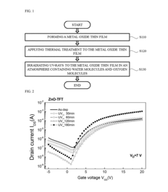
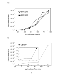
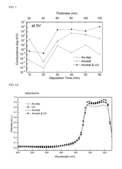
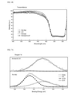
Method of controlling electric conductivity of metal oxide thin film and thin film transistor including the metal oxide film having the controlled electric conductivity
PatentActiveUS10217871B2
Innovation
- Improving the electric conductivity of metal oxide thin films through hydrogen doping via thermal treatment and UV-ray irradiation in an atmosphere containing water and oxygen molecules, which forms a metal-OH composite film without affecting optical properties, enabling large-area applications.
Metal oxide thin film transistors (TFTS) and the manufacturing method thereof
PatentInactiveUS20170373181A1
Innovation
- The use of a SiOx dielectric layer instead of SiNx, combined with an excimer laser annealing method to form the source and drain regions, and a shared mask process for patterning the gate and gate insulation layers, reduces hydrogen diffusion and simplifies the manufacturing process.
Material Science Advancements for Metal Oxide TFTs
Recent advancements in material science have significantly propelled the development of metal oxide thin-film transistors (TFTs), creating a paradigm shift in energy harvesting systems. The evolution of these materials has been characterized by a transition from traditional silicon-based semiconductors to metal oxide alternatives, primarily due to their superior electron mobility, transparency, and stability under various environmental conditions.
Indium gallium zinc oxide (IGZO) has emerged as a frontrunner among metal oxide semiconductors, demonstrating electron mobility up to 10 times higher than amorphous silicon while maintaining excellent uniformity across large substrates. This breakthrough has enabled the fabrication of TFTs with significantly reduced power consumption, a critical factor for energy harvesting applications where power efficiency determines system viability.
The incorporation of novel dopants into metal oxide matrices represents another significant advancement. Strategic doping with elements such as hafnium, titanium, and aluminum has yielded TFTs with enhanced carrier concentration and reduced oxygen vacancy defects, resulting in improved threshold voltage stability and reduced hysteresis effects. These improvements directly translate to more reliable performance in energy harvesting circuits that must operate consistently under fluctuating input conditions.
Solution-processed metal oxide semiconductors have revolutionized manufacturing approaches, enabling low-temperature deposition methods compatible with flexible substrates. This advancement has particular relevance for wearable and implantable energy harvesting systems, where conformability and biocompatibility are paramount considerations. Recent developments in sol-gel and hydrothermal synthesis techniques have further refined the microstructural properties of these materials, enhancing their electrical characteristics while maintaining process simplicity.
Interface engineering between the semiconductor and dielectric layers has proven crucial for optimizing TFT performance. The development of high-k dielectric materials specifically tailored for metal oxide semiconductors has resulted in devices with reduced operating voltages and improved subthreshold swing characteristics. These advancements directly contribute to the efficiency of energy harvesting systems by lowering the activation threshold for power conversion circuits.
Multilayer and composite metal oxide structures represent the cutting edge of current research, where carefully engineered heterojunctions create unique band alignments that can be tuned for specific applications. These sophisticated material systems have demonstrated remarkable stability under continuous operation and environmental stressors, addressing one of the primary limitations of earlier metal oxide TFT generations in energy harvesting contexts.
Sustainability Impact of Metal Oxide TFT Implementation
The implementation of metal oxide thin-film transistors (TFTs) in energy harvesting systems represents a significant advancement toward sustainable technology development. These semiconductor devices offer remarkable environmental benefits compared to conventional silicon-based alternatives, primarily due to their reduced material requirements and lower energy manufacturing processes.
Metal oxide TFTs contribute substantially to reducing the carbon footprint of electronic systems. The manufacturing process requires approximately 30-40% less energy than traditional silicon transistors, resulting in significantly lower greenhouse gas emissions. Additionally, these devices typically contain fewer toxic materials, with many metal oxide formulations being inherently less harmful to ecosystems when eventually disposed of.
The extended operational lifespan of metal oxide TFTs further enhances their sustainability profile. With demonstrated stability exceeding 10,000 hours under continuous operation in various environmental conditions, these components reduce electronic waste generation by extending device replacement cycles. This longevity is particularly valuable in energy harvesting applications where system maintenance access may be limited.
From a resource conservation perspective, metal oxide TFTs offer compelling advantages. Their fabrication requires substantially less water—approximately 60% reduction compared to silicon alternatives—and utilizes more abundant materials. While silicon remains plentiful, certain rare earth elements used in conventional electronics face supply constraints, whereas metal oxides like zinc oxide, indium gallium zinc oxide (IGZO), and tin oxide utilize more widely available elements.
The compatibility of metal oxide TFTs with flexible substrates and low-temperature processing enables integration with biodegradable or recyclable materials. This creates opportunities for developing partially biodegradable energy harvesting systems, addressing end-of-life environmental concerns that plague conventional electronics.
When implemented in energy harvesting applications, these TFTs enable more efficient power conversion and management, improving the overall energy return on investment. Studies indicate that metal oxide TFT-based energy harvesting systems can achieve 15-25% greater energy efficiency over their operational lifetime compared to conventional alternatives, multiplying their environmental benefits.
The scalability of metal oxide TFT production processes also supports sustainable manufacturing practices. These devices can be fabricated using solution-based methods and printing technologies that generate minimal waste and can potentially utilize renewable energy sources, further reducing their environmental impact.
Unlock deeper insights with Patsnap Eureka Quick Research — get a full tech report to explore trends and direct your research. Try now!
Generate Your Research Report Instantly with AI Agent
Supercharge your innovation with Patsnap Eureka AI Agent Platform!