Metal Oxide TFT’s Potential in Enhancing Device Miniaturization
SEP 28, 202510 MIN READ
Generate Your Research Report Instantly with AI Agent
Patsnap Eureka helps you evaluate technical feasibility & market potential.
Metal Oxide TFT Evolution and Objectives
Metal oxide thin-film transistors (TFTs) have emerged as a transformative technology in the electronics industry, evolving significantly since their initial development in the early 2000s. The journey began with amorphous silicon (a-Si) and polycrystalline silicon (poly-Si) TFTs dominating the market, but these technologies faced limitations in electron mobility and manufacturing complexity. The breakthrough came with the introduction of amorphous indium-gallium-zinc oxide (a-IGZO) TFTs around 2004, pioneered by researchers at Tokyo Institute of Technology, which offered superior electron mobility while maintaining low-temperature processing compatibility.
The evolution of metal oxide TFTs has been characterized by continuous improvements in material composition and fabrication techniques. Early iterations focused primarily on indium-based compounds, while recent developments have expanded to include more environmentally friendly and cost-effective alternatives such as zinc tin oxide (ZTO) and aluminum zinc oxide (AZO). This material diversification represents a critical trend in addressing sustainability concerns while maintaining performance standards.
Processing technologies have similarly advanced, transitioning from conventional vacuum-based deposition methods to solution-processing techniques that enable lower manufacturing costs and greater scalability. The implementation of atomic layer deposition (ALD) has further refined the precision of oxide semiconductor layers, allowing for unprecedented control over film thickness and composition at the atomic scale.
The miniaturization potential of metal oxide TFTs stems from their unique semiconductor properties. Unlike silicon-based technologies that require crystalline structures, metal oxide semiconductors can function effectively in an amorphous state, eliminating grain boundaries that typically limit scaling. This fundamental characteristic enables the creation of TFTs with channel lengths approaching sub-micron dimensions without significant performance degradation.
Current research objectives in the field are multifaceted, focusing on several key areas: reducing the operating voltage to enable compatibility with portable and wearable applications; enhancing stability under various environmental conditions; improving uniformity across large-area substrates; and developing complementary p-type oxide semiconductors to enable fully integrated oxide-based circuits.
The ultimate goal is to establish metal oxide TFTs as the foundation for next-generation display technologies, flexible electronics, and integrated sensor systems. This includes enabling higher resolution displays through smaller pixel sizes, creating more compact and energy-efficient wearable devices, and facilitating the integration of electronics into unconventional form factors and surfaces that were previously inaccessible with traditional silicon-based technologies.
As the industry moves toward increasingly miniaturized and specialized electronic systems, metal oxide TFTs are positioned to play a pivotal role in overcoming the physical and technical barriers that have historically limited device scaling and integration.
Market Demand for Miniaturized Electronics
The global market for miniaturized electronics continues to experience robust growth, driven primarily by consumer demand for smaller, lighter, and more powerful devices. This trend is particularly evident in smartphones, wearables, IoT devices, and medical implants where space constraints are critical design factors. Market research indicates that the miniaturized electronics sector is projected to grow at a compound annual growth rate (CAGR) of 15.3% through 2028, significantly outpacing the broader electronics industry.
Consumer electronics remains the largest segment demanding miniaturization technologies, with smartphones alone accounting for approximately 40% of the market value. The average smartphone now contains over 50 different sensors and semiconductor components, each under increasing pressure to reduce in size while improving performance. Industry surveys reveal that 78% of consumers consider device thickness and weight as important purchasing factors, creating direct market pressure for miniaturization technologies.
The healthcare sector represents the fastest-growing market segment for miniaturized electronics, with particular emphasis on implantable medical devices, point-of-care diagnostics, and wearable health monitors. The global market for miniaturized medical electronics is expected to reach $85 billion by 2027, with implantable devices showing the highest growth trajectory at 18.7% CAGR.
Industrial IoT applications are creating another significant demand vector for miniaturized components. As factories and supply chains deploy millions of sensors for monitoring and automation, the need for smaller, more energy-efficient electronics has intensified. Market analysis shows that industrial applications now account for 23% of the total miniaturized electronics market, up from just 12% five years ago.
The automotive industry has emerged as a major driver for miniaturization technologies, particularly with the acceleration of electric and autonomous vehicle development. Modern vehicles contain an average of 1,400 semiconductor chips, with premium models exceeding 3,000 components. The trend toward more sophisticated ADAS (Advanced Driver Assistance Systems) is creating particular demand for miniaturized sensing and processing components.
Supply chain constraints have highlighted the strategic importance of miniaturization technologies. Smaller components generally require less raw material, potentially reducing dependency on scarce resources and geopolitically sensitive supply chains. Industry reports indicate that manufacturers achieving 30% component size reduction can realize 15-25% material cost savings, creating additional market incentives beyond the primary functional benefits.
Current Status and Challenges in Metal Oxide TFT Technology
Metal oxide thin-film transistors (TFTs) have emerged as a promising technology for next-generation electronic devices, particularly in applications requiring miniaturization. Globally, significant advancements have been made in this field, with research institutions and companies in Asia, particularly Japan, South Korea, and Taiwan, leading development efforts. The United States and European countries have also contributed substantially to fundamental research and innovative applications.
Currently, metal oxide TFTs, especially those based on amorphous indium-gallium-zinc oxide (a-IGZO), have achieved commercial implementation in display technologies. These TFTs demonstrate electron mobility ranging from 5-20 cm²/Vs, significantly outperforming amorphous silicon (a-Si) TFTs while maintaining competitive production costs. The technology has successfully penetrated the market for large-area displays and is gradually expanding into flexible and transparent electronics.
Despite these achievements, several technical challenges persist. Stability issues under prolonged bias stress and environmental factors (humidity, temperature, light) remain significant concerns for widespread adoption. The performance degradation mechanisms are not fully understood, limiting the development of effective mitigation strategies. Additionally, achieving p-type metal oxide semiconductors with comparable performance to n-type counterparts continues to be a major hurdle for complementary circuit implementation.
Another critical challenge lies in scaling down device dimensions while maintaining electrical performance. As device sizes decrease below sub-micron levels, short-channel effects become more pronounced, affecting threshold voltage and subthreshold swing. The contact resistance at source/drain interfaces also becomes increasingly dominant as channel lengths shrink, impacting overall device performance.
Manufacturing challenges present additional obstacles. While metal oxide TFTs can be fabricated at relatively low temperatures (below 350°C), further reducing process temperatures without compromising performance is essential for integration with flexible substrates. Uniformity across large areas and batch-to-batch consistency remain problematic for mass production scenarios.
Material limitations also constrain advancement. The industry's heavy reliance on indium, a relatively scarce element, raises sustainability concerns. Research into alternative material systems that maintain comparable performance while using more abundant elements is ongoing but has yet to yield commercially viable solutions.
From a geographical perspective, Asia maintains technological leadership in production capabilities, while North America and Europe contribute significantly to fundamental research and novel applications. This distribution creates a complex ecosystem where innovation and commercialization often follow different geographical pathways, sometimes creating challenges in technology transfer and intellectual property management.
Current Miniaturization Solutions Using Metal Oxide TFTs
01 Advanced gate structure designs for miniaturization
Various gate structure designs can be implemented to achieve TFT device miniaturization. These include multi-gate structures, self-aligned gate configurations, and gate-all-around designs that provide better electrostatic control over the channel. These advanced gate architectures enable reduced channel lengths while maintaining good control over short-channel effects, allowing for smaller device footprints and higher integration density in metal oxide TFT technology.- Advanced gate structure designs for miniaturization: Various gate structure designs have been developed to reduce the size of metal oxide TFTs. These include multi-gate structures, self-aligned gates, and top-gate configurations that minimize the device footprint. These designs help improve the integration density while maintaining electrical performance. Advanced gate structures also enable better control of the channel, reducing short-channel effects that become prominent as devices shrink.
- Novel metal oxide semiconductor materials: The development of new metal oxide semiconductor materials has been crucial for TFT miniaturization. Materials such as IGZO, ZnO, and other multi-component oxides offer higher carrier mobility and better stability at smaller dimensions. These materials can be deposited using various techniques to achieve uniform thin films with precise thickness control, enabling the fabrication of smaller devices with improved performance characteristics.
- Vertical integration techniques: Vertical integration approaches have been implemented to reduce the lateral dimensions of metal oxide TFTs. By stacking device components vertically rather than horizontally, the overall footprint can be significantly reduced. These techniques include 3D stacking of transistors, vertical channel structures, and innovative contact arrangements that maximize space utilization while maintaining electrical connectivity between components.
- Advanced etching and patterning methods: Specialized etching and patterning techniques have been developed to achieve smaller feature sizes in metal oxide TFTs. These include high-resolution lithography, self-aligned processes, and selective etching methods that enable precise definition of device structures. These techniques help reduce the minimum feature size while maintaining the integrity of the metal oxide semiconductor layer, resulting in smaller devices with well-defined characteristics.
- Novel device architectures for size reduction: Innovative device architectures have been designed specifically for metal oxide TFT miniaturization. These include ultra-thin body structures, double-gate configurations, and fin-based designs that maximize the effective channel width while minimizing the overall device area. These architectures often incorporate specialized contact structures and isolation techniques to maintain performance while reducing dimensions, enabling higher integration density in display and integrated circuit applications.
02 Novel channel materials and stacked structures
Implementing novel metal oxide semiconductor materials and multi-layer channel structures can significantly contribute to TFT miniaturization. By using high-mobility oxide semiconductors such as IGZO, ZnO, or InOx-based compounds, and creating carefully engineered stacked channel structures, device performance can be maintained or improved while reducing physical dimensions. These materials enable thinner active layers and shorter channel lengths without compromising electrical characteristics.Expand Specific Solutions03 Source/drain engineering techniques
Advanced source/drain engineering techniques are crucial for metal oxide TFT miniaturization. These include implementing recessed source/drain structures, utilizing selective doping profiles, and developing low-resistance contact materials. By optimizing the source/drain regions, parasitic resistances can be reduced, allowing for shorter channel lengths and smaller device dimensions while maintaining good electrical performance and reliability.Expand Specific Solutions04 Vertical integration and 3D architectures
Vertical integration and 3D architectures represent a paradigm shift in metal oxide TFT miniaturization. By stacking devices vertically rather than spreading them horizontally, significant reductions in device footprint can be achieved. These approaches include vertical channel designs, 3D stacked structures, and innovative integration schemes that maximize the use of the vertical dimension, enabling higher device density and smaller overall circuit size.Expand Specific Solutions05 Advanced fabrication processes and materials
Advanced fabrication processes and materials play a critical role in metal oxide TFT miniaturization. These include high-resolution lithography techniques, atomic layer deposition for ultra-thin films, selective etching processes, and novel dielectric materials with high-k properties. These manufacturing innovations enable the creation of smaller feature sizes, thinner layers, and more precise structures, directly contributing to overall device miniaturization while maintaining or improving performance characteristics.Expand Specific Solutions
Leading Companies in Metal Oxide TFT Industry
Metal Oxide TFT technology is currently in a growth phase, with increasing adoption in display manufacturing due to its superior electron mobility and potential for device miniaturization. The global market is expanding rapidly, projected to reach significant scale as major players invest in research and production capabilities. Leading companies like BOE Technology, Samsung Display, and Sharp have achieved moderate to high technical maturity in metal oxide TFT implementation, particularly using IGZO technology. Semiconductor Energy Laboratory and Applied Materials are advancing the fundamental technology, while display manufacturers including TCL China Star, Japan Display, and Tianma Microelectronics are integrating these innovations into commercial products. Research institutions like Interuniversitair Micro-Electronica Centrum are collaborating with industry to overcome remaining technical challenges in stability and manufacturing scalability.
BOE Technology Group Co., Ltd.
Technical Solution: BOE has developed proprietary metal oxide TFT technology focused on high-resolution display applications with emphasis on miniaturization. Their approach utilizes modified IGZO compositions with carefully controlled oxygen vacancies to achieve balanced performance. BOE's technology incorporates unique passivation layers that significantly improve TFT stability under bias stress conditions, enabling smaller device geometries without reliability concerns. Their manufacturing process includes specialized annealing techniques that reduce defect states at the semiconductor-dielectric interface, allowing for channel lengths below 3μm while maintaining performance. BOE has successfully implemented these oxide TFTs in production for both LCD and OLED displays, achieving pixel circuits with significantly reduced footprint compared to conventional a-Si TFTs. Their recent advancements include multi-stacked oxide TFT structures that enable 3D integration of driving circuits, further reducing the lateral space requirements for display pixels.
Strengths: Highly optimized manufacturing processes enable cost-effective mass production while maintaining good device performance. Excellent integration with existing display manufacturing infrastructure allows for rapid adoption. Weaknesses: Electron mobility typically lower than some competitors (8-12 cm²/Vs range), potentially limiting switching speed in certain high-performance applications.
Semiconductor Energy Laboratory Co., Ltd.
Technical Solution: Semiconductor Energy Laboratory (SEL) has pioneered oxide semiconductor technology with their proprietary CAAC-IGZO (c-axis aligned crystalline indium-gallium-zinc oxide) TFTs. Their approach focuses on creating highly crystalline oxide structures that maintain excellent electron mobility while significantly reducing oxygen vacancy defects. SEL's technology enables transistors with channel lengths below 1μm while maintaining extremely low off-state leakage currents (10^-24 A/μm). Their CAAC-IGZO technology demonstrates remarkable stability under stress conditions, including light exposure, temperature variations, and voltage bias, making it suitable for ultra-miniaturized devices. SEL has successfully implemented this technology in flexible displays and ultra-low power memory applications, achieving bend radii below 1mm while maintaining electrical performance.
Strengths: Superior electron mobility (>10 cm²/Vs) combined with extremely low off-state current enables unprecedented power efficiency. Exceptional stability under environmental stressors allows for reliable operation in diverse conditions. Weaknesses: Manufacturing complexity of crystalline oxide structures requires specialized deposition equipment and precise process control, potentially increasing production costs compared to amorphous oxide semiconductors.
Key Patents and Innovations in Metal Oxide TFT Technology
Stability enhancements in metal oxide semiconductor thin film transistors
PatentWO2010074927A2
Innovation
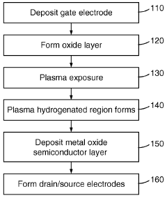
- Exposing the dielectric layer to a hydrogen-containing plasma before depositing the metal oxide semiconductor layer creates a hydrogenated region at the semiconductor-dielectric interface, enhancing carrier mobility and reducing hysteresis, thereby stabilizing the TFTs.
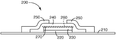
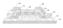
Metal oxide thin-film transistor, method of fabricating the same, and array substrate
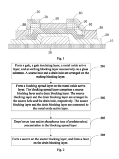
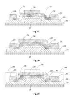
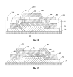
PatentInactiveUS9634036B1
Innovation
- A metal oxide TFT with a blocking spread layer doped with boron ions and/or phosphorus ions, composed of molybdenum and titanium, is used to prevent copper diffusion, with a thickness ranging from 100 to 500 Å and a doping concentration of 10% to 90%, which improves the blocking efficiency.
Material Science Advancements for Metal Oxide TFTs
Recent advancements in material science have significantly propelled the development of metal oxide thin-film transistors (TFTs), positioning them as key enablers for device miniaturization. The evolution of amorphous oxide semiconductors (AOS) has been particularly noteworthy, with indium-gallium-zinc-oxide (IGZO) emerging as a frontrunner due to its exceptional electron mobility characteristics and stability under various environmental conditions. These materials demonstrate electron mobilities typically ranging from 10-50 cm²/Vs, substantially outperforming traditional amorphous silicon (a-Si) which offers only 0.5-1 cm²/Vs.
Material engineering breakthroughs have focused on optimizing the composition and structure of metal oxide semiconductors. Researchers have successfully manipulated oxygen vacancy concentrations, a critical factor affecting carrier concentration and ultimately device performance. Advanced deposition techniques such as atomic layer deposition (ALD) and pulsed laser deposition (PLD) have enabled precise control over film thickness down to nanometer scales, facilitating the creation of ultra-thin active layers essential for miniaturized devices.
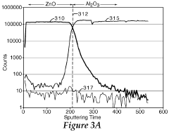
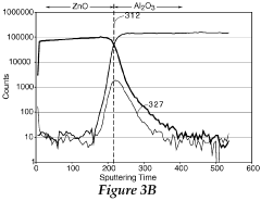
Interface engineering represents another crucial advancement area, addressing the semiconductor-dielectric interface quality that significantly impacts device performance. Novel high-k dielectric materials including hafnium oxide and aluminum oxide have been integrated with metal oxide semiconductors, resulting in improved gate control and reduced operating voltages. These developments directly contribute to scaling capabilities while maintaining electrical performance integrity.
Doping strategies have evolved to fine-tune the electrical properties of metal oxide TFTs. Strategic incorporation of elements such as hydrogen, nitrogen, and various metals has enabled customization of threshold voltages and carrier concentrations. This tailoring capability proves essential for diverse application requirements in miniaturized electronics, from low-power displays to high-performance logic circuits.
Multi-component oxide systems represent a promising frontier, where combinations of different metal oxides create semiconductor materials with enhanced stability and performance characteristics. These complex oxide systems demonstrate remarkable resilience against environmental factors and processing conditions, addressing reliability concerns in scaled-down devices.
Low-temperature processing techniques have expanded the application scope of metal oxide TFTs to temperature-sensitive substrates like flexible polymers. Solution-based deposition methods, including sol-gel processes and ink-jet printing, now enable fabrication at temperatures below 200°C without compromising electrical performance, opening pathways for flexible, lightweight miniaturized devices.
The integration of these material science advancements collectively addresses the fundamental challenges of device miniaturization, including short-channel effects, power consumption, and reliability concerns. As research continues to refine these materials and processing techniques, metal oxide TFTs are positioned to play an increasingly vital role in next-generation miniaturized electronic systems.
Material engineering breakthroughs have focused on optimizing the composition and structure of metal oxide semiconductors. Researchers have successfully manipulated oxygen vacancy concentrations, a critical factor affecting carrier concentration and ultimately device performance. Advanced deposition techniques such as atomic layer deposition (ALD) and pulsed laser deposition (PLD) have enabled precise control over film thickness down to nanometer scales, facilitating the creation of ultra-thin active layers essential for miniaturized devices.
Interface engineering represents another crucial advancement area, addressing the semiconductor-dielectric interface quality that significantly impacts device performance. Novel high-k dielectric materials including hafnium oxide and aluminum oxide have been integrated with metal oxide semiconductors, resulting in improved gate control and reduced operating voltages. These developments directly contribute to scaling capabilities while maintaining electrical performance integrity.
Doping strategies have evolved to fine-tune the electrical properties of metal oxide TFTs. Strategic incorporation of elements such as hydrogen, nitrogen, and various metals has enabled customization of threshold voltages and carrier concentrations. This tailoring capability proves essential for diverse application requirements in miniaturized electronics, from low-power displays to high-performance logic circuits.
Multi-component oxide systems represent a promising frontier, where combinations of different metal oxides create semiconductor materials with enhanced stability and performance characteristics. These complex oxide systems demonstrate remarkable resilience against environmental factors and processing conditions, addressing reliability concerns in scaled-down devices.
Low-temperature processing techniques have expanded the application scope of metal oxide TFTs to temperature-sensitive substrates like flexible polymers. Solution-based deposition methods, including sol-gel processes and ink-jet printing, now enable fabrication at temperatures below 200°C without compromising electrical performance, opening pathways for flexible, lightweight miniaturized devices.
The integration of these material science advancements collectively addresses the fundamental challenges of device miniaturization, including short-channel effects, power consumption, and reliability concerns. As research continues to refine these materials and processing techniques, metal oxide TFTs are positioned to play an increasingly vital role in next-generation miniaturized electronic systems.
Manufacturing Scalability and Cost Considerations
The manufacturing scalability of metal oxide TFTs represents a critical advantage in their potential for device miniaturization. Unlike traditional silicon-based technologies that require complex and expensive fabrication processes, metal oxide TFTs can be manufactured using relatively simpler deposition techniques such as sputtering and solution processing. This fundamental difference enables production at lower temperatures, significantly reducing energy consumption and associated costs in the manufacturing pipeline.
Large-area fabrication capabilities present another compelling advantage for metal oxide TFT technology. The ability to deposit uniform metal oxide films across substantial substrate areas facilitates economies of scale that are particularly beneficial for mass production scenarios. This scalability has been demonstrated in the display industry, where IGZO (Indium Gallium Zinc Oxide) TFTs have been successfully implemented in commercial products ranging from smartphones to large-format televisions.
Cost considerations reveal a nuanced picture when comparing metal oxide TFTs with competing technologies. While the initial material costs for certain metal oxides (particularly those containing indium) can be relatively high due to resource scarcity, the overall manufacturing economics remain favorable. This advantage stems from reduced process complexity, lower thermal budget requirements, and higher production yields. Industry analyses suggest that the total cost of ownership for metal oxide TFT production lines can be 15-30% lower than comparable silicon-based alternatives when factoring in equipment, energy, and maintenance expenses.
The compatibility of metal oxide TFTs with existing manufacturing infrastructure represents another significant economic advantage. Many facilities currently producing amorphous silicon TFTs can be retrofitted to accommodate metal oxide TFT production with relatively modest capital investments. This transition pathway reduces barriers to adoption and accelerates market penetration for this emerging technology.
Yield considerations also favor metal oxide TFTs in the context of miniaturization. As device dimensions decrease, the uniformity advantages of metal oxide semiconductors become increasingly valuable. Studies indicate that metal oxide TFT production can maintain higher yields at smaller feature sizes compared to alternatives, particularly in flexible or non-planar form factors where traditional technologies struggle with consistency across the substrate.
Future manufacturing innovations are expected to further enhance the cost-effectiveness of metal oxide TFT production. Developments in atmospheric pressure processing, roll-to-roll fabrication techniques, and direct printing methods show particular promise for reducing capital equipment requirements and enabling truly high-volume, low-cost manufacturing paradigms that will be essential for widespread adoption in miniaturized device applications.
Unlock deeper insights with Patsnap Eureka Quick Research — get a full tech report to explore trends and direct your research. Try now!
Generate Your Research Report Instantly with AI Agent
Supercharge your innovation with Patsnap Eureka AI Agent Platform!