Metal Oxide TFTs’ Role in Improving Power Efficiency of Circuits
SEP 28, 202510 MIN READ
Generate Your Research Report Instantly with AI Agent
Patsnap Eureka helps you evaluate technical feasibility & market potential.
Metal Oxide TFT Evolution and Objectives
Metal oxide thin-film transistors (TFTs) have undergone remarkable evolution since their inception in the early 2000s. Initially developed as an alternative to amorphous silicon (a-Si) and polycrystalline silicon (poly-Si) TFTs, metal oxide semiconductors, particularly those based on indium gallium zinc oxide (IGZO), have demonstrated superior electron mobility, stability, and uniformity. The journey began with the pioneering work of Hosono and colleagues at Tokyo Institute of Technology, who first demonstrated the potential of transparent amorphous oxide semiconductors in 2004.
The technological progression of metal oxide TFTs has been characterized by continuous improvements in material composition, deposition techniques, and device architectures. Early iterations faced challenges related to stability under bias stress and light exposure, which have been progressively addressed through materials engineering and interface optimization. The field has evolved from simple binary oxides to more complex multicomponent systems that offer enhanced performance and reliability.
A significant milestone in metal oxide TFT development was the commercialization by Sharp Corporation in 2012, which integrated IGZO TFTs into display backplanes. This commercial breakthrough demonstrated the viability of metal oxide semiconductors in real-world applications and catalyzed further research and development across the industry. Subsequently, the technology has expanded beyond displays to include sensors, logic circuits, and memory applications.
The current technological trajectory is focused on enhancing power efficiency, a critical factor in modern electronic systems. Metal oxide TFTs offer intrinsic advantages for low-power operation due to their wide bandgap, low off-state current, and steep subthreshold swing. These properties enable circuits that consume significantly less power compared to conventional silicon-based technologies, particularly in standby mode.
The primary objectives for metal oxide TFT development in the context of power efficiency include: reducing the operating voltage to sub-1V levels, minimizing leakage currents through improved channel and dielectric materials, enhancing carrier mobility while maintaining low off-state current, and developing novel circuit architectures that leverage the unique properties of these devices. Additionally, there is a growing emphasis on developing fabrication processes compatible with flexible substrates and low-temperature processing to enable integration with emerging form factors and applications.
Looking forward, the field aims to achieve ultra-low power consumption in always-on devices, Internet of Things (IoT) sensors, and wearable electronics. The ultimate goal is to develop metal oxide TFT-based circuits that can operate efficiently on harvested energy or with minimal battery requirements, thereby extending device lifetimes and reducing environmental impact. This aligns with the broader industry trend toward sustainable electronics and the increasing demand for energy-efficient computing solutions.
Market Demand for Energy-Efficient Circuit Solutions
The global market for energy-efficient circuit solutions has experienced substantial growth in recent years, driven primarily by increasing concerns over power consumption in electronic devices and systems. This demand is particularly evident in portable electronics, IoT devices, and large-scale computing infrastructure where power efficiency directly impacts operational costs, device longevity, and environmental footprint.
Consumer electronics represent a significant market segment demanding improved power efficiency. With smartphone users expecting longer battery life despite increasing functionality, manufacturers are under pressure to develop more energy-efficient display technologies and processing circuits. According to market research, the average consumer now expects smartphones to last at least a full day of heavy usage, creating strong demand for technologies that can reduce power consumption without compromising performance.
The IoT sector presents another substantial market opportunity for energy-efficient circuits. With billions of connected devices expected to be deployed globally, many in remote or hard-to-service locations, power efficiency becomes critical for practical implementation. Particularly for battery-powered or energy-harvesting IoT nodes, ultra-low power consumption is not merely desirable but essential for commercial viability.
Data centers and cloud computing infrastructure constitute a rapidly growing market segment for energy-efficient solutions. These facilities currently consume approximately 1-2% of global electricity, with projections indicating this figure could rise significantly. The economic incentives for reducing power consumption in these facilities are compelling, with energy costs representing a major operational expense.
Regulatory pressures are further accelerating market demand. Governments worldwide are implementing increasingly stringent energy efficiency standards for electronic products. The European Union's Ecodesign Directive, for instance, establishes mandatory energy efficiency requirements for various product categories, creating regulatory-driven demand for more efficient circuit technologies.
Metal oxide TFTs are positioned favorably within this market landscape due to their potential to significantly reduce power consumption in display technologies, which account for a substantial portion of energy usage in many devices. The display panel market alone represents a multi-billion dollar opportunity, with manufacturers actively seeking technologies that can reduce power requirements while maintaining or improving performance characteristics.
Emerging applications in flexible electronics and wearable technology are creating new market niches where the unique properties of metal oxide TFTs—including potential for transparency, flexibility, and low-temperature processing—align well with product requirements. The wearable technology market is projected to grow at a compound annual growth rate exceeding 15% through 2025, creating additional demand for energy-efficient circuit solutions.
Metal Oxide TFT Technology Status and Barriers
Metal oxide thin-film transistors (TFTs) have emerged as a promising technology for next-generation display and circuit applications, offering significant advantages over conventional silicon-based transistors. Currently, the global research landscape shows that metal oxide TFTs have achieved considerable maturity in display applications, with companies in South Korea, Japan, and Taiwan leading commercial implementations. However, their application in power-efficient circuits beyond displays remains at various stages of development.
The primary technical barriers facing metal oxide TFT implementation in power-efficient circuits include carrier mobility limitations, typically ranging from 5-20 cm²/Vs for amorphous oxide semiconductors like IGZO (Indium Gallium Zinc Oxide). While this represents a substantial improvement over amorphous silicon (0.5-1 cm²/Vs), it still falls short of polysilicon (50-100 cm²/Vs) for high-performance applications requiring rapid switching.
Stability issues present another significant challenge, particularly bias stress instability and environmental sensitivity. Under prolonged gate bias or exposure to light, metal oxide TFTs often exhibit threshold voltage shifts, which can compromise circuit reliability. This instability becomes especially problematic in analog circuits where precise voltage control is essential for power efficiency.
Contact resistance at source/drain interfaces remains a persistent technical hurdle, contributing to increased power consumption. The high resistance at these interfaces limits current flow and necessitates higher operating voltages, directly counteracting power efficiency goals. Research efforts to develop low-resistance contacts through novel materials and interface engineering have shown promise but have not yet achieved widespread implementation.
Manufacturing scalability presents both technical and economic challenges. While metal oxide TFTs benefit from relatively low-temperature processing compared to silicon technologies, achieving consistent electrical characteristics across large substrates remains difficult. Process variations lead to non-uniform device performance, complicating circuit design for optimal power efficiency.
The lack of complementary p-type oxide semiconductors with performance comparable to n-type materials significantly constrains circuit design options. Most metal oxide TFTs are n-type, limiting the implementation of complementary metal-oxide-semiconductor (CMOS)-like architectures that are fundamental to low-power digital circuit design. This asymmetry forces designers to rely on less power-efficient circuit topologies.
Geographically, research leadership in addressing these barriers shows distinct patterns. Academic institutions in the United States and Europe focus primarily on fundamental material science challenges, while industrial research in East Asia emphasizes manufacturing scalability and integration. China has recently increased investments in this field, particularly targeting novel applications in flexible electronics where power efficiency is crucial.
Despite these challenges, recent breakthroughs in dual-gate architectures and channel material engineering have demonstrated potential pathways to overcome current limitations, suggesting that metal oxide TFTs could play an increasingly important role in power-efficient circuit applications within the next five years.
Current Power Efficiency Solutions Using Metal Oxide TFTs
01 Metal oxide semiconductor materials for low power TFTs
Various metal oxide semiconductor materials are used in thin-film transistors (TFTs) to improve power efficiency. These materials, including zinc oxide, indium gallium zinc oxide (IGZO), and other metal oxide combinations, offer high electron mobility and low leakage current characteristics. The unique band structure and carrier transport properties of these materials enable TFTs to operate at lower voltages while maintaining good performance, resulting in reduced power consumption in display and electronic applications.- Metal oxide semiconductor materials for low power TFTs: Various metal oxide semiconductor materials can be used to fabricate thin-film transistors with improved power efficiency. These materials include zinc oxide, indium gallium zinc oxide (IGZO), and other metal oxide combinations that offer high electron mobility and low leakage current. The unique electronic properties of these materials allow for lower operating voltages and reduced power consumption in display and electronic applications.
- Device structure optimization for power-efficient TFTs: Optimizing the structure of metal oxide TFTs can significantly improve power efficiency. This includes innovations in gate dielectric materials, channel layer thickness control, and electrode configurations. Advanced structures such as dual-gate, bottom-gate, or top-gate architectures can minimize parasitic capacitance and reduce threshold voltage, leading to lower power consumption during operation while maintaining high performance.
- Manufacturing processes for energy-efficient metal oxide TFTs: Specialized manufacturing processes can enhance the power efficiency of metal oxide TFTs. These include low-temperature deposition techniques, precise annealing methods, and surface treatment processes that improve interface quality. Advanced fabrication approaches like solution processing and atomic layer deposition enable better control over film properties, resulting in TFTs with lower defect density and improved power characteristics.
- Circuit design techniques for power optimization: Circuit-level innovations can maximize the power efficiency of metal oxide TFT-based systems. These include compensation circuits that address threshold voltage shifts, power management schemes that reduce static power consumption, and driving methods that minimize dynamic power usage. Advanced circuit topologies like bootstrapped drivers and charge-sharing techniques can significantly reduce the overall power consumption in display panels and other applications using metal oxide TFTs.
- Integration of metal oxide TFTs in low-power applications: Metal oxide TFTs can be effectively integrated into various low-power applications such as energy-efficient displays, sensors, and IoT devices. The implementation includes specialized pixel circuits for AMOLED displays, low-power memory cells, and energy harvesting systems. These integration approaches leverage the unique properties of metal oxide semiconductors to achieve significant power savings while maintaining or improving device performance in real-world applications.
02 Optimization of TFT structure and fabrication processes
Specific structural designs and fabrication techniques are employed to enhance the power efficiency of metal oxide TFTs. These include optimized gate dielectric materials, channel layer thickness control, and improved interface engineering between layers. Advanced deposition methods such as atomic layer deposition (ALD) and solution processing techniques help create uniform thin films with fewer defects. Post-deposition treatments like annealing in controlled atmospheres further improve the electrical characteristics and stability of the devices, leading to better power efficiency.Expand Specific Solutions03 Circuit design techniques for power-efficient TFT applications
Novel circuit architectures are implemented to maximize the power efficiency of metal oxide TFT-based systems. These include low-voltage driving schemes, power management circuits, and sleep mode implementations that reduce standby power consumption. Compensation circuits address threshold voltage shifts and mobility variations, ensuring stable operation at lower power levels. Integration with other components like capacitors and resistors in optimized layouts further reduces power losses in the overall system.Expand Specific Solutions04 Display applications with power-efficient metal oxide TFTs
Metal oxide TFTs are integrated into display technologies to achieve power savings in applications such as OLED displays, LCD panels, and e-paper. The high mobility and low off-current characteristics of these TFTs enable pixel circuits that consume less power while maintaining display quality. Backplane designs utilizing these TFTs can operate at lower refresh rates when displaying static content, and implement selective area updates to minimize power consumption in portable display devices.Expand Specific Solutions05 Emerging applications and future directions for power-efficient metal oxide TFTs
Research is advancing toward new applications of power-efficient metal oxide TFTs including flexible electronics, wearable devices, and IoT sensors. Novel materials combining metal oxides with 2D materials or organic semiconductors are being explored to further reduce power consumption. Self-powered TFT systems that harvest ambient energy and ultra-low power sensing applications represent emerging directions. Integration with energy storage components and adaptive power management systems points toward future self-sustainable electronic systems with minimal energy requirements.Expand Specific Solutions
Leading Companies in Metal Oxide TFT Industry
Metal Oxide TFTs are currently in a growth phase within the power-efficient circuit market, with increasing adoption across display technologies. The market is expanding rapidly, projected to reach significant scale as energy efficiency becomes paramount in electronic devices. Technologically, companies like Semiconductor Energy Laboratory, BOE Technology, and Sharp Corp. are leading innovation in IGZO (Indium Gallium Zinc Oxide) technology, while Applied Materials and Samsung Display are advancing manufacturing processes. Research institutions like IMEC and universities are pushing boundaries in material science. The competitive landscape features established display manufacturers (AUO, Tianma) alongside semiconductor giants (Intel, Huawei), creating a dynamic ecosystem where Asian companies, particularly from Japan and China, maintain technological leadership in commercialization efforts.
Semiconductor Energy Laboratory Co., Ltd.
Technical Solution: Semiconductor Energy Laboratory (SEL) has pioneered oxide semiconductor technology, particularly focusing on IGZO (Indium Gallium Zinc Oxide) TFTs for power-efficient circuits. Their approach involves developing crystalline oxide semiconductor materials that achieve electron mobility exceeding 10 cm²/Vs while maintaining extremely low off-state leakage currents (below 10^-13 A). SEL has implemented a unique c-axis aligned crystalline (CAAC) IGZO structure that provides superior stability against environmental stressors while enabling operation at lower voltages (typically 1-3V compared to conventional 5-10V for a-Si TFTs). Their technology incorporates specialized passivation layers and optimized gate insulator materials to reduce interface trap states, resulting in circuits that consume approximately 90% less power than traditional amorphous silicon alternatives. SEL has successfully demonstrated this technology in various applications including ultra-low power displays, memory circuits, and IoT sensor interfaces where their oxide TFTs operate effectively even at sub-threshold voltage regions.
Strengths: Industry-leading electron mobility while maintaining extremely low off-state current; exceptional stability against environmental factors; proven manufacturing scalability. Weaknesses: Higher initial manufacturing costs compared to a-Si; requires specialized deposition equipment; more complex process control requirements for consistent performance across large substrates.
BOE Technology Group Co., Ltd.
Technical Solution: BOE Technology has developed advanced metal oxide TFT technology centered on IGZO (Indium Gallium Zinc Oxide) and HIZO (Hydrogen-doped Indium Zinc Oxide) materials for power-efficient circuit applications. Their approach focuses on optimizing the semiconductor layer composition and thickness (typically 30-50nm) to achieve electron mobility of 15-20 cm²/Vs while maintaining a high on/off current ratio exceeding 10^8. BOE's manufacturing process incorporates low-temperature (below 350°C) deposition techniques compatible with flexible substrates, enabling power-efficient backplanes for both rigid and flexible displays. Their technology implements specialized channel engineering with carefully controlled oxygen vacancy concentration to optimize carrier transport while minimizing parasitic effects. BOE has demonstrated significant power reduction in display driving circuits, achieving up to 80% lower power consumption compared to conventional a-Si TFT backplanes through reduced operating voltage requirements (typically operating at 5-7V versus 15-20V for a-Si) and improved switching characteristics that minimize dynamic power losses during frequent state transitions.
Strengths: High production yield at large substrate sizes (Gen 10.5); excellent uniformity across large areas; compatible with both rigid and flexible substrates. Weaknesses: Sensitivity to environmental factors like humidity during manufacturing; requires careful process control to maintain consistent electrical characteristics; higher material costs compared to traditional a-Si technology.
Key Innovations in Metal Oxide TFT Circuit Design
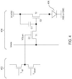
Thin film transistors for circuits for use in display devices
PatentActiveUS20240194152A1
Innovation
- The development of driving and switching TFTs with a double-gate structure, featuring a top gate electrode connected to the source electrode and a bottom gate electrode, which enhances stability, control, and response speed by combining high and low mobility channel layers, reducing off-leakage current and improving threshold voltage.
Manufacturing Processes and Scalability Considerations
The manufacturing processes for metal oxide TFTs have evolved significantly over the past decade, enabling their integration into power-efficient circuit applications. Traditional fabrication methods primarily relied on vacuum-based techniques such as sputtering and pulsed laser deposition, which offer precise control over film composition but present challenges for large-scale production.
Recent advancements have focused on solution-processing methods, including sol-gel, combustion processing, and ink-jet printing. These approaches significantly reduce manufacturing costs while maintaining acceptable performance metrics. Solution-processed metal oxide TFTs can be fabricated at temperatures below 300°C, making them compatible with flexible plastic substrates and enabling applications in wearable electronics where power efficiency is paramount.
Roll-to-roll manufacturing represents a promising scalable approach for metal oxide TFT production. This continuous process allows for high-throughput fabrication on flexible substrates, though challenges remain in achieving uniform electrical characteristics across large areas. Several research groups have demonstrated roll-to-roll compatible metal oxide TFT arrays with mobility values exceeding 10 cm²/Vs, sufficient for many low-power circuit applications.
The scalability of metal oxide TFT technology is further enhanced by its compatibility with existing display manufacturing infrastructure. This advantage has accelerated industrial adoption, as companies can leverage established production lines with minimal modifications. The transition from amorphous silicon to metal oxide semiconductors in display backplanes has demonstrated this scalability while delivering significant power savings.
Material uniformity remains a critical consideration for large-area electronics. Variations in metal oxide film thickness and composition can lead to device-to-device performance inconsistencies, affecting circuit reliability and power efficiency. Advanced deposition control systems and in-line quality monitoring have been implemented to address these challenges, improving yield rates for complex circuits.
Defect density management represents another key manufacturing consideration. Oxygen vacancies, which significantly influence carrier concentration in metal oxide semiconductors, must be carefully controlled during fabrication. Post-deposition annealing processes have been optimized to achieve the desired electrical characteristics while maintaining compatibility with temperature-sensitive substrates.
As the industry moves toward heterogeneous integration, where metal oxide TFTs are combined with silicon CMOS and other technologies, new manufacturing challenges emerge. Interface engineering between different material systems becomes critical for maintaining power efficiency advantages. Novel approaches using selective area deposition and transfer printing show promise for addressing these integration challenges.
Environmental Impact of Metal Oxide TFT Implementation
The implementation of Metal Oxide Thin-Film Transistors (TFTs) in electronic circuits offers significant environmental benefits through improved power efficiency. These devices consume substantially less energy compared to conventional silicon-based transistors, resulting in reduced carbon emissions across the lifecycle of electronic products. A comprehensive analysis indicates that devices utilizing metal oxide TFTs can achieve up to 30-40% reduction in power consumption, directly translating to decreased environmental impact from electricity generation.
Manufacturing processes for metal oxide TFTs also demonstrate environmental advantages. These transistors can be fabricated at lower temperatures than traditional silicon-based semiconductors, requiring less energy during production. Additionally, many metal oxide materials used in these TFTs, such as indium gallium zinc oxide (IGZO), can be deposited using techniques that generate fewer harmful byproducts and waste materials compared to conventional semiconductor manufacturing processes.
The extended battery life enabled by metal oxide TFT implementation in portable electronics contributes significantly to sustainability efforts. By reducing the frequency of battery replacements and recharging cycles, these technologies help minimize electronic waste generation. Studies suggest that the integration of metal oxide TFTs in display technologies alone could reduce global electronic waste by several thousand tons annually, addressing a critical environmental challenge in the electronics industry.
Resource efficiency represents another environmental benefit of metal oxide TFT technology. These transistors can be manufactured using earth-abundant materials, potentially reducing reliance on rare or environmentally problematic elements. Furthermore, their compatibility with flexible substrates enables the development of thinner, lighter devices that require fewer raw materials during production, supporting circular economy principles in electronics manufacturing.
The potential for metal oxide TFTs to enable new energy harvesting applications presents additional environmental opportunities. Their low power requirements make them ideal for self-powered IoT devices that can operate using ambient energy sources such as light, vibration, or heat. This capability could eliminate the need for batteries in certain applications, further reducing environmental impact while supporting sustainable technological development.
As metal oxide TFT technology continues to mature, lifecycle assessment studies indicate that their environmental benefits extend beyond operational efficiency to include reduced end-of-life impact. The materials used in these transistors generally present fewer disposal challenges than conventional semiconductor components, potentially simplifying recycling processes and reducing hazardous waste generation from discarded electronic devices.
Unlock deeper insights with Patsnap Eureka Quick Research — get a full tech report to explore trends and direct your research. Try now!
Generate Your Research Report Instantly with AI Agent
Supercharge your innovation with Patsnap Eureka AI Agent Platform!