Examining Metal Oxide TFT Patent Trends in Electronics
SEP 28, 20259 MIN READ
Generate Your Research Report Instantly with AI Agent
Patsnap Eureka helps you evaluate technical feasibility & market potential.
Metal Oxide TFT Evolution and Research Objectives
Metal oxide thin-film transistors (TFTs) have emerged as a transformative technology in the electronics industry over the past two decades. The evolution of this technology can be traced back to the early 2000s when researchers began exploring alternatives to amorphous silicon (a-Si) and polycrystalline silicon (poly-Si) TFTs due to their inherent limitations in mobility and stability. The breakthrough came in 2004 when Hosono and his team at Tokyo Institute of Technology demonstrated the first high-performance amorphous oxide semiconductor (AOS) TFT using indium gallium zinc oxide (IGZO).
The technological trajectory of metal oxide TFTs has been characterized by continuous improvements in material composition, deposition techniques, and device architectures. From the initial IGZO formulations, the field has expanded to include various metal oxide combinations such as zinc tin oxide (ZTO), indium zinc oxide (IZO), and hafnium indium zinc oxide (HIZO), each offering specific advantages in terms of mobility, stability, or processing compatibility.
Patent analysis reveals a clear trend toward industrialization beginning around 2010, with companies like Sharp, Samsung, and LG Display filing significant intellectual property related to manufacturing processes and integration schemes. This period marked the transition from laboratory curiosity to commercial viability, culminating in the first consumer products featuring metal oxide TFT backplanes in 2012.
Current research objectives in the metal oxide TFT domain focus on several key areas. First, enhancing carrier mobility beyond 50 cm²/Vs while maintaining excellent uniformity across large substrates remains a primary goal for enabling next-generation display technologies. Second, improving stability under various stress conditions (bias, illumination, temperature) continues to be critical for long-term device reliability.
The development of low-temperature processing routes (below 200°C) represents another significant research direction, aimed at enabling flexible and conformable electronics on polymer substrates. Additionally, there is growing interest in environmentally friendly compositions that reduce or eliminate scarce elements like indium, addressing sustainability concerns in the supply chain.
From a manufacturing perspective, research objectives include simplifying the fabrication process to reduce production costs, developing solution-processing methods for roll-to-roll manufacturing, and improving compatibility with existing display production infrastructure. The ultimate goal is to position metal oxide TFT technology as the dominant backplane solution for advanced display technologies including OLED, microLED, and next-generation sensing arrays.
Market Analysis for Metal Oxide TFT Applications
The metal oxide thin-film transistor (TFT) market has experienced significant growth in recent years, driven primarily by increasing demand for high-resolution displays in consumer electronics. The global market for metal oxide TFTs reached approximately $3.2 billion in 2022 and is projected to grow at a compound annual growth rate (CAGR) of 12.8% through 2028, potentially reaching $6.5 billion by the end of the forecast period.
Display applications currently dominate the metal oxide TFT market, accounting for over 75% of total demand. Within this segment, OLED displays represent the fastest-growing application area due to their superior performance characteristics and increasing adoption in premium smartphones and televisions. The transition from amorphous silicon (a-Si) to metal oxide semiconductors, particularly IGZO (Indium Gallium Zinc Oxide), has been accelerated by consumer preferences for higher resolution, lower power consumption, and thinner form factors in display devices.
Geographically, East Asia continues to lead the market with approximately 68% of global production capacity, with South Korea, Japan, and Taiwan serving as manufacturing hubs. However, China has been rapidly expanding its production capabilities, with substantial investments in new fabrication facilities dedicated to metal oxide TFT production.
Beyond displays, emerging applications in sensors, logic circuits, and memory devices are creating new market opportunities. The healthcare sector shows particular promise, with metal oxide TFTs being integrated into flexible biosensors and medical imaging equipment. This diversification is expected to reduce market dependency on consumer electronics cycles and provide more stable growth trajectories.
Supply chain considerations have become increasingly important following recent global disruptions. The reliance on rare elements like indium has prompted research into alternative material compositions, with zinc tin oxide (ZTO) and aluminum zinc oxide (AZO) gaining attention as potentially more sustainable and cost-effective alternatives.
Customer segmentation reveals that premium device manufacturers represent the primary market for metal oxide TFTs, though mid-range product integration is accelerating as production costs decrease. Enterprise and industrial applications are growing at 18% annually, outpacing consumer electronics, suggesting a broadening market base beyond traditional consumer products.
Market barriers include high initial capital requirements for production facilities and technical challenges in scaling production while maintaining performance consistency. These factors have contributed to market concentration among established manufacturers with significant R&D capabilities and existing fabrication infrastructure.
Global Metal Oxide TFT Development Status and Barriers
Metal oxide thin-film transistor (TFT) technology has emerged as a critical component in modern display and electronics industries, offering significant advantages over traditional amorphous silicon (a-Si) TFTs. Currently, the global development of metal oxide TFTs is characterized by rapid advancement but with notable regional disparities. Asia, particularly Japan, South Korea, and Taiwan, leads in both research output and commercial implementation, with companies like Sharp, Samsung, and LG Display holding substantial patent portfolios and manufacturing capabilities.
The current technical maturity of metal oxide TFTs varies across applications. In display technologies, particularly for large-area LCD and OLED panels, metal oxide TFTs have achieved commercial viability with indium gallium zinc oxide (IGZO) being the dominant material composition. However, in emerging applications such as flexible electronics, transparent displays, and integrated circuit applications, the technology remains in earlier development stages with significant challenges to overcome.
Key technical barriers currently impeding wider adoption include stability issues under environmental stressors (temperature, humidity, and light), particularly for zinc oxide-based TFTs which exhibit threshold voltage shifts under prolonged bias stress. Manufacturing scalability presents another significant challenge, as uniform deposition of metal oxide semiconductors over large areas requires precise control of process parameters that is difficult to maintain in high-volume production environments.
Material limitations constitute another major barrier, with the scarcity and cost of indium raising concerns about long-term sustainability. Research into alternative material systems such as zinc tin oxide (ZTO) shows promise but has not yet achieved the performance levels of IGZO. Additionally, the integration of metal oxide TFTs with other electronic components in complex circuits faces compatibility challenges with existing manufacturing processes.
From a geographical perspective, intellectual property barriers have created a fragmented development landscape. Japanese and Korean companies hold dominant positions in fundamental patents, creating entry barriers for new market participants. European research institutions have made significant contributions to fundamental understanding of metal oxide semiconductor physics, while North American companies have focused more on specialized applications and integration technologies.
The environmental impact of metal oxide TFT manufacturing processes represents an emerging concern, with regulatory barriers potentially affecting future development trajectories. Water usage, chemical waste, and energy consumption in fabrication processes are receiving increased scrutiny, driving research into more sustainable manufacturing approaches and materials.
Current Metal Oxide TFT Patent Solutions
01 Metal oxide semiconductor materials for TFTs
Various metal oxide semiconductor materials are used in thin-film transistors (TFTs) to achieve specific electrical properties. These materials include indium gallium zinc oxide (IGZO), zinc oxide (ZnO), and other metal oxide combinations that offer advantages such as high electron mobility, good stability, and transparency. The selection of metal oxide materials significantly impacts the performance characteristics of the TFT, including switching speed, power consumption, and reliability.- Metal oxide semiconductor materials for TFTs: Various metal oxide semiconductor materials can be used in thin-film transistors (TFTs) to achieve desired electrical properties. These materials include indium gallium zinc oxide (IGZO), zinc oxide (ZnO), indium oxide, and other metal oxide combinations. The selection of metal oxide materials affects key transistor parameters such as carrier mobility, threshold voltage, and stability, making them suitable for different display and electronic applications.
- Fabrication methods for metal oxide TFTs: Various fabrication techniques are employed to create metal oxide TFTs with optimized performance. These methods include sputtering, atomic layer deposition (ALD), solution processing, and annealing treatments. The fabrication process significantly impacts the crystallinity, defect density, and interface quality of the metal oxide layer, which in turn affects the electrical characteristics and reliability of the resulting TFTs.
- TFT device structures and configurations: Different structural configurations of metal oxide TFTs can be implemented to enhance performance characteristics. These include bottom-gate, top-gate, dual-gate, and vertical structures. Each configuration offers specific advantages in terms of electrical performance, manufacturing complexity, and integration capability with other components. The choice of structure depends on the intended application and desired performance metrics.
- Integration of metal oxide TFTs in display technologies: Metal oxide TFTs are widely integrated into various display technologies including LCD, OLED, and flexible displays. Their high electron mobility, good uniformity, and low leakage current make them particularly suitable for driving pixels in high-resolution displays. The integration process involves specific design considerations to ensure compatibility with display backplanes and to achieve desired visual performance.
- Performance enhancement techniques for metal oxide TFTs: Various techniques are employed to enhance the performance of metal oxide TFTs. These include interface engineering, doping strategies, passivation layers, and multi-layer channel structures. These approaches aim to improve stability, reduce threshold voltage shift, enhance carrier mobility, and extend device lifetime. Advanced processing techniques and novel material combinations continue to push the performance boundaries of metal oxide TFTs.
02 TFT structure and fabrication methods
Various structural designs and fabrication methods are employed for metal oxide TFTs to optimize performance. These include bottom-gate, top-gate, and dual-gate configurations, each offering different advantages in terms of electrical characteristics and manufacturing complexity. Advanced fabrication techniques such as low-temperature processing, solution-based deposition, and patterning methods enable the production of high-performance TFTs on various substrates, including flexible materials.Expand Specific Solutions03 Performance enhancement techniques
Various techniques are employed to enhance the performance of metal oxide TFTs. These include channel engineering, interface modification, and doping strategies to improve carrier mobility, reduce threshold voltage, and enhance stability. Additional approaches involve passivation layers to protect against environmental factors, annealing treatments to optimize crystal structure, and multi-layer channel designs to achieve desired electrical characteristics.Expand Specific Solutions04 Applications in display technologies
Metal oxide TFTs are widely used in display technologies due to their excellent electrical properties and optical transparency. They serve as switching and driving elements in active-matrix displays, including OLED and LCD panels. The high electron mobility of metal oxide TFTs enables high-resolution, fast-response displays with reduced power consumption. Their application extends to transparent displays, flexible displays, and large-area display panels.Expand Specific Solutions05 Stability and reliability improvements
Enhancing the stability and reliability of metal oxide TFTs is crucial for long-term device performance. Various approaches address issues such as bias stress instability, light sensitivity, and environmental degradation. These include specialized passivation layers, optimized gate dielectrics, and compositional modifications of the metal oxide semiconductor. Additional techniques involve hydrogen or oxygen management within the device structure to control defect states and improve operational stability.Expand Specific Solutions
Leading Companies and Competitive Landscape
The metal oxide TFT market is currently in a growth phase, with an expanding global market driven by increasing demand for high-performance displays in consumer electronics, automotive interfaces, and medical devices. The technology has reached moderate maturity, with key players like Semiconductor Energy Laboratory, BOE Technology, and Samsung Display leading innovation through extensive patent portfolios. Japanese companies (Sharp, Japan Display) and Chinese manufacturers (TCL China Star, Tianma) are aggressively expanding their technological capabilities, while research institutions like South China University of Technology contribute to fundamental advancements. The competitive landscape shows regional clusters of expertise in East Asia, with emerging competition from specialized players focusing on novel applications in flexible electronics and transparent displays, indicating a dynamic market with significant growth potential.
Semiconductor Energy Laboratory Co., Ltd.
Technical Solution: Semiconductor Energy Laboratory (SEL) has pioneered oxide semiconductor technology, particularly focusing on IGZO (Indium Gallium Zinc Oxide) TFTs. Their technical approach involves creating highly stable metal oxide semiconductors with optimized oxygen vacancy control. SEL has developed proprietary crystallization techniques that enhance electron mobility while maintaining low off-state current characteristics. Their patented technologies include specialized annealing processes that reduce defect states at the semiconductor-insulator interface, resulting in TFTs with mobility exceeding 10 cm²/Vs while maintaining excellent threshold voltage stability[1]. SEL has also innovated in multilayer oxide semiconductor structures that combine different metal oxide compositions to achieve complementary device performance. Their recent patents focus on back-channel treatment methods that significantly improve device reliability under negative bias temperature stress conditions, extending operational lifetimes by orders of magnitude compared to conventional a-Si TFTs[3].
Strengths: Industry-leading expertise in oxide semiconductor physics with exceptional stability and reliability metrics. Their devices show minimal threshold voltage shift even after extended stress testing. Weaknesses: Manufacturing processes often require more complex deposition and annealing steps compared to conventional technologies, potentially increasing production costs and limiting mass-market adoption.
BOE Technology Group Co., Ltd.
Technical Solution: BOE has developed advanced metal oxide TFT technologies focused on large-area display applications. Their technical approach centers on industrialization of IGZO and other metal oxide semiconductors for high-resolution displays. BOE's patented technologies include specialized sputtering methods for uniform large-area deposition with precise stoichiometry control across Gen 10.5 substrates. They've pioneered low-temperature processing techniques that enable oxide TFT fabrication on flexible substrates at temperatures below 200°C while maintaining mobility values above 15 cm²/Vs[2]. BOE has also developed proprietary passivation layer technologies that significantly enhance environmental stability, particularly against moisture and oxygen contamination. Their recent innovations include self-aligned top-gate structures that reduce parasitic capacitance, enabling faster pixel switching for high refresh rate displays. BOE has further patented unique compensation circuit designs specifically optimized for oxide TFT backplanes that address threshold voltage variation issues inherent to large-area manufacturing[4].
Strengths: Exceptional manufacturing scale capabilities with demonstrated ability to mass-produce oxide TFT backplanes for commercial display products. Their technologies show excellent uniformity across large substrates. Weaknesses: Some of their oxide TFT implementations show higher sensitivity to light-induced instability compared to competitors, requiring additional compensation circuitry in high-performance applications.
Key Patent Analysis and Technical Innovations
Metal oxide thin-film transistor, method of fabricating the same, and array substrate
PatentInactiveUS9634036B1
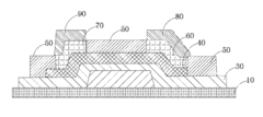
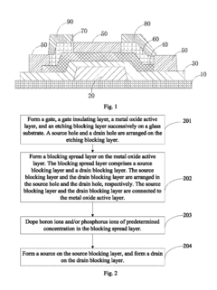
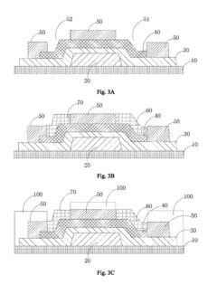
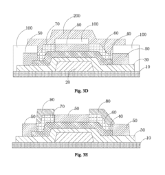
Innovation
- A metal oxide TFT with a blocking spread layer doped with boron ions and/or phosphorus ions, composed of molybdenum and titanium, is used to prevent copper diffusion, with a thickness ranging from 100 to 500 Å and a doping concentration of 10% to 90%, which improves the blocking efficiency.
Thin film transistor
PatentActiveUS20150069379A1
Innovation
- A thin film transistor with an indium gallium zinc oxide (IGZO) semiconductor layer, where the atomic ratios of gallium to indium and zinc are optimized between 1.5 to 2, enhancing the stability and reliability by maintaining mobility greater than 10 cm2/Vs and reducing threshold voltage variation to less than 1.3 V, and subthreshold swing to less than 0.6 V/dec.
IP Strategy and Patent Portfolio Management
In the rapidly evolving landscape of metal oxide TFT technology, strategic intellectual property management has become a critical factor for companies seeking competitive advantage. Effective IP strategy requires a comprehensive understanding of the patent landscape, including identification of white spaces, potential infringement risks, and opportunities for cross-licensing.
Companies leading in metal oxide TFT development typically employ multi-layered patent portfolio strategies. These strategies often include filing patents across the entire value chain—from basic materials and manufacturing processes to device structures and end applications. This approach creates a protective barrier around core technologies while establishing potential licensing revenue streams.
Patent mapping reveals distinct patterns in metal oxide TFT IP ownership. Major display manufacturers like Samsung, LG Display, and Sharp hold substantial portfolios focused on implementation technologies, while research institutions and materials companies tend to control fundamental patents related to novel oxide semiconductors and their properties. This distribution creates a complex ecosystem where strategic partnerships and licensing agreements become essential for market access.
Geographic filing strategies show interesting trends, with companies increasingly filing patents in emerging manufacturing hubs like China and Vietnam, beyond traditional markets like Japan, South Korea, and the United States. This reflects the shifting landscape of electronics manufacturing and the growing importance of these regions in the global supply chain.
Freedom-to-operate (FTO) analysis has become increasingly important as the metal oxide TFT patent landscape becomes more crowded. Companies must navigate carefully to avoid infringement while developing differentiated technologies. Strategic patent acquisition through M&A activities has emerged as a common approach to rapidly strengthen IP positions in this field.
Defensive patenting strategies are also prevalent, with companies filing patents not necessarily for direct implementation but to prevent competitors from gaining exclusive rights to adjacent technologies. This creates a complex web of overlapping claims that requires sophisticated IP management to navigate effectively.
For new entrants to the metal oxide TFT market, developing a strategic patent portfolio often involves identifying underexplored niches or application areas where novel IP can be generated without directly competing with established players. This approach allows for market entry while minimizing IP conflicts with industry leaders.
Environmental Impact and Sustainability Considerations
The environmental footprint of metal oxide TFT technology represents a critical consideration as this technology continues to proliferate across the electronics industry. Manufacturing processes for metal oxide semiconductors typically require fewer steps and lower processing temperatures compared to traditional silicon-based technologies, resulting in reduced energy consumption during production. This energy efficiency advantage translates to lower carbon emissions throughout the manufacturing lifecycle, positioning metal oxide TFTs as a comparatively sustainable option in display and semiconductor technologies.
Recent patent trends reveal increasing focus on environmentally friendly manufacturing processes for metal oxide TFTs. Innovations in solution-processing methods that minimize the use of toxic chemicals and reduce waste generation have gained significant traction. These advancements align with global sustainability initiatives and increasingly stringent environmental regulations governing electronics manufacturing.
Material composition presents both challenges and opportunities for sustainability. While indium, a common component in IGZO (Indium Gallium Zinc Oxide) TFTs, faces supply constraints and environmental concerns related to mining practices, patent activity shows growing interest in alternative material systems. Zinc-tin oxide and aluminum-based compounds are emerging as promising substitutes that reduce dependence on rare or environmentally problematic elements.
End-of-life considerations have become increasingly prominent in metal oxide TFT patent filings. Designs that facilitate easier disassembly and material recovery are gaining attention as electronic waste management becomes a global priority. Patents addressing recyclability and reduced toxic material content demonstrate the industry's response to circular economy principles and extended producer responsibility regulations.
Energy efficiency during device operation represents another significant environmental advantage. Metal oxide TFTs typically require lower operating voltages than conventional technologies, contributing to reduced power consumption in finished electronic products. This characteristic is particularly valuable for battery-powered devices, where energy efficiency directly impacts battery life and resource utilization.
The integration of metal oxide TFTs in flexible and wearable electronics presents additional sustainability benefits through potential device longevity. Patents focusing on mechanical durability and resistance to environmental degradation suggest pathways to extended product lifecycles, potentially reducing electronic waste generation. These innovations align with sustainable design principles that prioritize durability and repairability over disposability.
Unlock deeper insights with Patsnap Eureka Quick Research — get a full tech report to explore trends and direct your research. Try now!
Generate Your Research Report Instantly with AI Agent
Supercharge your innovation with Patsnap Eureka AI Agent Platform!