Metal Oxide TFTs and Their Contribution to Sustainable Electronics
SEP 28, 20259 MIN READ
Generate Your Research Report Instantly with AI Agent
Patsnap Eureka helps you evaluate technical feasibility & market potential.
Metal Oxide TFT Evolution and Objectives
Metal oxide thin-film transistors (TFTs) have emerged as a transformative technology in the electronics industry, evolving significantly since their initial development in the early 2000s. The journey began with amorphous silicon (a-Si) TFTs dominating the display industry, followed by the introduction of polycrystalline silicon (poly-Si) TFTs offering improved performance. However, the breakthrough came with the development of amorphous oxide semiconductors (AOS), particularly indium gallium zinc oxide (IGZO), which combined high electron mobility with low-temperature processing capabilities.
The evolution of metal oxide TFTs has been driven by the increasing demand for high-performance, energy-efficient, and flexible electronic devices. Early research focused primarily on zinc oxide (ZnO) based TFTs, which demonstrated promising electrical properties but suffered from stability issues. The incorporation of additional metal elements like indium and gallium led to the development of more stable and higher-performing IGZO TFTs, which have since become commercially viable for various applications.
A significant milestone in metal oxide TFT development was achieved in 2004 when researchers at Tokyo Institute of Technology demonstrated room-temperature fabrication of transparent TFTs using amorphous IGZO. This breakthrough opened doors for applications in transparent electronics and flexible displays, areas previously limited by the high-temperature processing requirements of conventional silicon-based technologies.
The primary technical objectives in metal oxide TFT research have evolved to address several key challenges. These include enhancing carrier mobility to improve switching speed and current drive capability, reducing threshold voltage instability for consistent performance, developing low-temperature fabrication processes compatible with flexible substrates, and minimizing environmental impact through sustainable materials and manufacturing methods.
Current research is increasingly focused on sustainability aspects, aiming to reduce or eliminate rare and toxic elements like indium while maintaining high performance. This has led to exploration of alternative metal oxide compositions using abundant elements such as zinc-tin oxide (ZTO) and aluminum-zinc oxide (AZO). Additionally, there is growing interest in biodegradable substrates and environmentally friendly processing techniques to minimize the ecological footprint of electronic devices.
Looking forward, the technical roadmap for metal oxide TFTs aims to achieve ultra-low power consumption, enhanced stability under various environmental conditions, and compatibility with emerging technologies such as printed electronics and Internet of Things (IoT) devices. The ultimate goal is to develop metal oxide TFT technology that not only offers superior performance but also contributes significantly to sustainable electronics through reduced energy consumption, longer device lifetimes, and environmentally responsible manufacturing processes.
Market Analysis for Sustainable Electronics
The sustainable electronics market is experiencing significant growth driven by increasing environmental awareness and regulatory pressures. Currently valued at approximately $76 billion globally, this sector is projected to reach $115 billion by 2028, with a compound annual growth rate of 8.7%. Metal oxide thin-film transistors (TFTs) are positioned as a key enabling technology within this expanding market due to their superior environmental profile compared to conventional silicon-based semiconductors.
Consumer electronics represents the largest application segment for sustainable electronics, accounting for nearly 40% of the market share. Within this segment, display technologies incorporating metal oxide TFTs, particularly those using indium gallium zinc oxide (IGZO), have gained substantial traction. These displays offer reduced power consumption of up to 30% compared to traditional amorphous silicon alternatives, directly addressing consumer demand for longer battery life in portable devices.
The healthcare sector presents the fastest-growing opportunity for sustainable electronics, with projected growth rates exceeding 12% annually through 2028. Medical wearables and monitoring devices benefit significantly from metal oxide TFT technology's flexibility, biocompatibility, and low power requirements. These attributes enable the development of biodegradable or recyclable medical sensors that minimize electronic waste while maintaining clinical efficacy.
Regional analysis reveals Asia-Pacific as the dominant market for sustainable electronics manufacturing, controlling approximately 65% of global production capacity for metal oxide TFT-based devices. However, Europe leads in adoption rates for sustainable electronics products, driven by stringent environmental regulations and consumer preferences. The European Green Deal has established ambitious targets for electronic waste reduction, creating market pull for technologies like metal oxide TFTs that facilitate device recyclability.
Supply chain considerations reveal both opportunities and challenges. The reduced material complexity of metal oxide TFTs compared to silicon alternatives offers potential for more localized production with shorter supply chains. However, concerns regarding indium availability persist, as this critical element faces potential supply constraints with reserves concentrated in China, South Korea, and Japan.
Price sensitivity analysis indicates that while sustainable electronics currently command a premium of 15-25% over conventional alternatives, this gap is narrowing as production scales and technologies mature. Metal oxide TFT manufacturing costs have decreased by approximately 40% over the past five years, approaching cost parity with amorphous silicon in certain applications, particularly for large-area displays and sensor arrays.
Current Status and Barriers in Metal Oxide TFT Technology
Metal oxide thin-film transistors (TFTs) have emerged as a promising technology in the field of sustainable electronics, with significant advancements achieved globally. Currently, indium gallium zinc oxide (IGZO) and zinc oxide (ZnO) based TFTs dominate commercial applications, particularly in display technologies. These materials offer superior electron mobility compared to amorphous silicon, typically achieving 5-15 cm²/Vs in production environments, while maintaining excellent uniformity across large substrates.
Despite these achievements, several technical challenges persist in metal oxide TFT technology. The most significant barrier remains the development of stable p-type metal oxide semiconductors with comparable performance to their n-type counterparts. This asymmetry limits the creation of complementary metal oxide semiconductor (CMOS) circuits, which are essential for low-power applications. Current p-type oxides such as SnO and Cu₂O exhibit mobilities below 5 cm²/Vs and suffer from stability issues in ambient conditions.
Another critical challenge is the long-term stability of metal oxide TFTs under bias stress and environmental factors. Threshold voltage shifts occur during prolonged operation, particularly under negative bias illumination stress (NBIS), affecting device reliability. These instabilities are attributed to oxygen vacancy dynamics and charge trapping at semiconductor-dielectric interfaces, requiring further fundamental understanding and material engineering solutions.
Manufacturing scalability presents additional hurdles. While vacuum-based deposition techniques like sputtering and atomic layer deposition produce high-quality films, they involve high capital costs and energy consumption. Solution-processing methods offer more sustainable alternatives but currently yield devices with inferior performance and reproducibility compared to vacuum-processed counterparts.
Geographically, research and development in metal oxide TFT technology is concentrated in East Asia, particularly Japan, South Korea, and Taiwan, where major display manufacturers have established production capabilities. European research institutions focus on fundamental material science and novel applications, while North American efforts are primarily directed toward next-generation computing applications and integration with emerging technologies.
The supply chain for critical materials poses another constraint, as indium—a key component in high-performance oxide semiconductors—faces potential scarcity and price volatility. This has accelerated research into indium-free alternatives such as zinc tin oxide (ZTO) and aluminum zinc oxide (AZO), though these materials currently exhibit lower performance metrics.
Environmental considerations also present challenges, as conventional fabrication processes involve hazardous chemicals and high-temperature annealing steps. Recent efforts have focused on developing low-temperature processes compatible with flexible substrates and environmentally benign precursors, though these approaches require further optimization to match the performance of traditional methods.
Contemporary Metal Oxide TFT Implementation Approaches
01 Metal oxide semiconductor materials for TFTs
Various metal oxide semiconductor materials can be used in thin-film transistors (TFTs) to achieve specific electrical properties. These materials include zinc oxide (ZnO), indium gallium zinc oxide (IGZO), and other metal oxide combinations that offer advantages such as high electron mobility, good stability, and transparency. The selection of appropriate metal oxide materials is crucial for optimizing TFT performance in display and electronic applications.- Metal oxide semiconductor materials for TFTs: Various metal oxide semiconductor materials are used in thin-film transistors (TFTs) to achieve specific electrical properties. These materials include zinc oxide (ZnO), indium gallium zinc oxide (IGZO), and other metal oxide combinations that offer advantages such as high electron mobility, good stability, and transparency. The selection of metal oxide materials significantly impacts the performance characteristics of the TFTs, including switching speed, power consumption, and reliability.
- Fabrication methods for metal oxide TFTs: Various fabrication techniques are employed to manufacture metal oxide TFTs, including sputtering, atomic layer deposition (ALD), solution processing, and chemical vapor deposition (CVD). These methods control the crystallinity, composition, and interface quality of the metal oxide layers. Post-deposition treatments such as annealing in different atmospheres help optimize the electrical properties and stability of the devices. Advanced patterning techniques enable the creation of high-resolution TFT structures for display and integrated circuit applications.
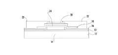
- Device structures and architectures for metal oxide TFTs: Metal oxide TFTs can be fabricated in various structural configurations including bottom-gate, top-gate, staggered, and coplanar architectures. Each structure offers different advantages in terms of performance, manufacturing complexity, and integration capability. Multi-layer channel structures using combinations of different metal oxides can enhance electrical characteristics. Advanced device architectures incorporate features like dual gates, self-aligned structures, or embedded passivation layers to improve stability and reduce parasitic effects.
- Integration of metal oxide TFTs in display technologies: Metal oxide TFTs are widely integrated into display technologies such as OLED, LCD, and microLED displays. Their high electron mobility enables faster pixel switching and higher resolution displays. The transparency of metal oxide semiconductors allows for the development of transparent displays. These TFTs can be fabricated on flexible substrates, enabling bendable and rollable display applications. The integration process includes specialized pixel circuits, driving schemes, and compensation techniques to ensure uniform display performance.
- Performance enhancement and stability improvement techniques: Various methods are employed to enhance the performance and stability of metal oxide TFTs. These include interface engineering between the semiconductor and dielectric layers, passivation techniques to protect against environmental factors, and doping strategies to control carrier concentration. Bias stress stability is improved through specialized annealing processes and compositional optimization. Additional techniques include the incorporation of buffer layers, hydrogen management, and defect control to minimize threshold voltage shifts and improve long-term reliability under operational conditions.
02 Fabrication methods for metal oxide TFTs
Various fabrication techniques are employed to manufacture metal oxide TFTs, including sputtering, atomic layer deposition, solution processing, and thermal annealing. These methods affect the crystallinity, interface quality, and overall performance of the TFTs. Optimized fabrication processes can reduce defects, improve carrier mobility, and enhance the stability of metal oxide TFT devices for commercial applications.Expand Specific Solutions03 Device structures and architectures for metal oxide TFTs
Different structural configurations can be implemented in metal oxide TFTs, including bottom-gate, top-gate, staggered, and coplanar architectures. Each structure offers specific advantages in terms of performance, manufacturing complexity, and integration capabilities. Advanced device architectures may incorporate additional features such as dual gates, self-aligned structures, or specialized contact configurations to enhance electrical characteristics and reliability.Expand Specific Solutions04 Integration of metal oxide TFTs in display technologies
Metal oxide TFTs are widely integrated into display technologies such as OLED, LCD, and flexible displays. Their high electron mobility, transparency, and low-temperature processing compatibility make them ideal for driving pixels in display panels. The integration process involves specific design considerations to optimize pixel circuits, reduce power consumption, and improve display performance while maintaining manufacturing yield.Expand Specific Solutions05 Performance enhancement and stability improvement techniques
Various methods are employed to enhance the performance and stability of metal oxide TFTs, including interface engineering, passivation layers, doping strategies, and bias stress compensation. These techniques address common challenges such as threshold voltage shifts, hysteresis, and degradation under prolonged operation. Implementing appropriate enhancement methods can significantly improve device reliability, operational lifetime, and electrical characteristics for commercial applications.Expand Specific Solutions
Leading Companies and Research Institutions in Metal Oxide Semiconductors
Metal Oxide TFTs are emerging as a key technology in sustainable electronics, with the market currently in a growth phase characterized by increasing adoption across display and sensor applications. The global market is expanding rapidly, projected to reach significant scale as manufacturers seek energy-efficient, high-performance alternatives to conventional silicon-based transistors. Companies like BOE Technology, TCL China Star, and Applied Materials are leading commercial deployment, while Semiconductor Energy Laboratory and Sharp Corp. have established strong intellectual property positions through pioneering research. Academic institutions such as South China University of Technology and Indian Institute of Technology Madras are advancing fundamental research. The technology has reached moderate maturity for display applications, with companies like JOLED and Flexterra pushing boundaries in flexible electronics, though challenges remain in standardization and manufacturing scalability for next-generation applications.
BOE Technology Group Co., Ltd.
Technical Solution: BOE has developed a comprehensive metal oxide TFT technology platform focused on environmental sustainability and performance optimization. Their approach utilizes high-mobility IGZO and zinc oxide-based semiconductors deposited through optimized sputtering processes that reduce target material consumption by approximately 25% compared to conventional methods. BOE has implemented a unique multi-layer oxide stack architecture that enhances carrier mobility while maintaining low off-state current, enabling both high-performance and low-power applications. Their manufacturing process incorporates reduced-temperature annealing techniques (below 350°C) that decrease energy consumption while improving TFT stability. BOE has also pioneered the integration of metal oxide TFTs with advanced backplane designs for flexible and transparent displays, utilizing environmentally friendly substrate materials. Their recent innovations include oxide TFT backplanes that reduce display power consumption by up to 30% through optimized pixel circuits and driving schemes, contributing significantly to end-product sustainability.
Strengths: Vertically integrated manufacturing capabilities from materials to finished displays; advanced process optimization for high-volume production; strong implementation in commercial products across multiple display technologies. Weaknesses: Relatively high defect sensitivity requiring stringent process control; challenges in achieving consistent performance across very large substrates; ongoing optimization needed for flexible applications.
Applied Materials, Inc.
Technical Solution: Applied Materials has developed comprehensive manufacturing solutions specifically for metal oxide TFT production, focusing on sustainability and efficiency. Their approach centers on advanced Physical Vapor Deposition (PVD) systems that enable precise control of metal oxide film composition and thickness uniformity across large substrates. Their AKT-PiVot DT PVD system allows for multi-layer deposition of various metal oxide combinations (including IGZO, ZnO, and SnO variants) with reduced material waste compared to conventional systems. Applied Materials has also pioneered low-temperature plasma-enhanced chemical vapor deposition (PECVD) processes for gate insulators that interface optimally with oxide semiconductors, reducing interface trap states and improving TFT stability. Their integrated manufacturing approach incorporates in-line metrology and advanced process control to maximize yield while minimizing energy consumption and material usage. Recent innovations include equipment designs that reduce process gas consumption by up to 40% and energy usage by approximately 30% compared to previous generations.
Strengths: End-to-end manufacturing solutions that optimize material utilization and energy efficiency; advanced process control capabilities that maximize yield; equipment designed specifically for large-area electronics production. Weaknesses: High capital investment requirements for manufacturers; complex integration challenges when implementing new material systems; dependence on specialized gases and materials that may have their own sustainability challenges.
Key Patents and Scientific Breakthroughs in Metal Oxide TFTs
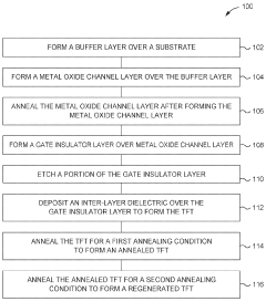
Regeneration anneal of metal oxide thin-film transistors
PatentWO2023224792A1
Innovation
- A method involving the formation of a buffer layer, a metal oxide channel layer, and an inter-layer dielectric, followed by a two-stage annealing process at specific temperature ranges (first annealing at 250°C or greater and second annealing at 150°C to 275°C) to regenerate TFTs with improved threshold voltage and stability, regardless of integration process.
Metal oxide thin film transistor with excellent temperature stability
PatentInactiveJP2016502278A
Innovation
- Implementing a passivation material with a conduction band at least 0.5 eV higher than the metal oxide semiconductor's conduction band to transfer electrons away from the interface, reducing oxygen loss and improving stability by selecting materials like Ta2O5, TiO2, or other insulating oxides that are less susceptible to reduction.
Environmental Impact Assessment of Metal Oxide TFT Manufacturing
The manufacturing processes of Metal Oxide Thin-Film Transistors (TFTs) present both environmental challenges and opportunities for sustainable electronics. Traditional semiconductor manufacturing typically involves energy-intensive processes and hazardous materials, but metal oxide TFTs offer several comparative advantages from an environmental perspective.
Metal oxide TFT production generally requires lower processing temperatures (200-300°C) compared to conventional silicon-based technologies (>900°C), resulting in significantly reduced energy consumption during manufacturing. This temperature difference translates to approximately 30-40% energy savings across the production lifecycle, contributing to lower carbon emissions in the electronics supply chain.
Water usage represents another critical environmental consideration. Metal oxide TFT fabrication typically consumes 25-35% less ultrapure water than traditional silicon semiconductor manufacturing. This reduction is particularly significant given that a conventional semiconductor facility may use 2-4 million gallons of water daily, making water conservation a substantial sustainability benefit.
Regarding material toxicity, metal oxide TFTs generally utilize less hazardous substances compared to technologies that rely heavily on arsenic or gallium arsenide. Common metal oxides like IGZO (Indium Gallium Zinc Oxide) contain fewer toxic elements, though concerns remain regarding indium extraction and its limited natural abundance. Recent research has focused on developing indium-free alternatives using more abundant elements like zinc tin oxide (ZTO) to address resource scarcity concerns.
Waste generation during manufacturing presents ongoing challenges. The etching processes used in metal oxide TFT production generate acidic waste streams that require proper treatment. However, the overall waste volume is typically 15-20% lower than in conventional silicon semiconductor manufacturing due to simpler device structures and fewer processing steps.
End-of-life considerations reveal additional environmental advantages. The simpler material composition of metal oxide TFTs potentially facilitates easier recycling and material recovery compared to complex multilayer silicon devices. This characteristic becomes increasingly important as electronic waste volumes continue to grow globally at 3-5% annually.
Life cycle assessments indicate that metal oxide TFT-based displays can reduce the overall carbon footprint by 20-30% compared to conventional technologies when considering the entire product lifecycle from material extraction through manufacturing, use, and disposal. This improvement stems from both manufacturing efficiencies and reduced energy consumption during device operation.
Circular Economy Integration Strategies for TFT Production
The integration of circular economy principles into Metal Oxide TFT production represents a critical pathway toward sustainable electronics manufacturing. Current linear production models—extracting raw materials, manufacturing components, and disposing of products at end-of-life—are increasingly unsustainable given resource constraints and environmental impacts. Metal oxide TFT production can pioneer circular approaches through several strategic interventions.
Material selection optimization stands as a foundational strategy, with manufacturers increasingly selecting materials based on their recyclability and reusability profiles. Indium-free alternatives like zinc tin oxide (ZTO) reduce dependence on scarce elements while maintaining performance characteristics. These alternative materials often require lower processing temperatures, further reducing energy consumption during manufacturing.
Design for disassembly represents another crucial approach, where TFT components are engineered from the outset to facilitate easy separation at end-of-life. This includes modular designs, standardized components, and avoiding permanent adhesives that complicate recycling processes. Such design considerations enable more efficient material recovery and component reuse.
Manufacturing process innovations have emerged that minimize waste generation and energy consumption. Additive manufacturing techniques like inkjet printing of metal oxide semiconductors significantly reduce material waste compared to traditional subtractive processes. Solution-based deposition methods operate at lower temperatures, decreasing energy requirements while enabling the use of biodegradable substrates.
Closed-loop supply chains are being established through industry collaborations, where manufacturers partner with recyclers and material suppliers to create systems for recovering and reprocessing end-of-life TFT components. These partnerships facilitate the return of valuable materials to production cycles, reducing virgin material demand.
Extended producer responsibility programs incentivize manufacturers to take ownership of their products throughout the entire lifecycle. Leading electronics companies now implement take-back schemes for displays containing metal oxide TFTs, ensuring proper recycling and material recovery.
Technological innovations in recycling are advancing the feasibility of circular approaches. New hydrometallurgical processes can recover over 90% of metal oxides from discarded TFTs with significantly lower energy requirements than traditional methods. These processes preserve the functional properties of recovered materials, enabling their reintroduction into high-quality applications rather than downcycling.
The transition toward circular economy integration in metal oxide TFT production requires coordinated effort across the value chain but promises substantial sustainability benefits, including reduced environmental impact, resource conservation, and potentially lower production costs through material recovery and reuse.
Unlock deeper insights with Patsnap Eureka Quick Research — get a full tech report to explore trends and direct your research. Try now!
Generate Your Research Report Instantly with AI Agent
Supercharge your innovation with Patsnap Eureka AI Agent Platform!