The Role of Metal Oxide TFTs in Advancing Smart Grid Technology
SEP 28, 202510 MIN READ
Generate Your Research Report Instantly with AI Agent
Patsnap Eureka helps you evaluate technical feasibility & market potential.
Metal Oxide TFTs Evolution and Smart Grid Integration Goals
Metal oxide thin-film transistors (TFTs) have evolved significantly over the past two decades, transforming from laboratory curiosities to commercially viable technologies with diverse applications. The journey began in the early 2000s with the development of amorphous indium gallium zinc oxide (a-IGZO) TFTs, which demonstrated superior electron mobility compared to traditional amorphous silicon alternatives. This breakthrough enabled the creation of higher-performance, lower-power electronic devices that could be manufactured using existing production infrastructure.
The technological evolution of metal oxide TFTs has been characterized by continuous improvements in material composition, deposition techniques, and device architectures. Early challenges related to stability and uniformity have been progressively addressed through innovations in passivation layers, interface engineering, and annealing processes. Recent advancements have focused on enhancing flexibility, transparency, and environmental stability, making these devices increasingly suitable for integration into smart grid components.
Smart grid technology represents a modernized electrical grid that uses digital communications and automation to monitor and control power flows, enabling more efficient and reliable electricity distribution. The integration of metal oxide TFTs into smart grid systems aims to address several critical challenges in the current infrastructure, including real-time monitoring capabilities, distributed intelligence, and energy efficiency optimization.
A primary goal of this integration is to develop advanced sensing networks that can provide granular data on grid conditions. Metal oxide TFTs offer advantages in this context due to their low power consumption, high switching speeds, and potential for integration with various sensor technologies. These characteristics make them ideal for deployment in remote monitoring stations and intelligent electronic devices throughout the distribution network.
Another significant objective is the enhancement of grid resilience through improved power electronics. Metal oxide TFTs can enable more efficient power conversion and switching operations, potentially reducing energy losses in the transmission and distribution system. Their ability to operate at higher frequencies than silicon-based alternatives may also contribute to more compact and efficient power management systems.
Looking forward, the convergence of metal oxide TFT technology with smart grid infrastructure presents opportunities for transformative innovations in energy management. Research trends indicate growing interest in developing self-powered sensor nodes using energy harvesting techniques, where the low power requirements of metal oxide TFTs provide a distinct advantage. Additionally, the potential for large-area, flexible electronics based on these materials could enable new form factors for grid monitoring and control devices that can be deployed in previously inaccessible locations.
Market Demand Analysis for Smart Grid Semiconductor Solutions
The smart grid semiconductor market is experiencing robust growth driven by the global transition toward more efficient, reliable, and sustainable energy systems. Current market analysis indicates that the smart grid semiconductor sector is valued at approximately $12 billion, with projections suggesting a compound annual growth rate of 8.5% through 2030. This growth is primarily fueled by increasing electricity demand, aging grid infrastructure requiring modernization, and governmental policies promoting renewable energy integration.
Metal oxide thin-film transistors (TFTs) are emerging as critical components within this expanding market. Their unique properties—including high electron mobility, excellent stability, and low-temperature processing capabilities—position them as ideal solutions for next-generation grid management systems. The demand for these semiconductor solutions is particularly strong in advanced metering infrastructure, where global deployments are expected to reach 1.3 billion units by 2026.
Utility companies represent the largest customer segment, accounting for approximately 45% of market demand. These organizations are increasingly investing in grid modernization to improve operational efficiency and reduce transmission losses, which currently average 8-15% in developing markets. The industrial sector follows at 30% of market share, driven by energy management needs and the growing adoption of distributed energy resources.
Regionally, North America leads the market with a 35% share, followed by Europe (28%) and Asia-Pacific (25%). However, the Asia-Pacific region is demonstrating the fastest growth rate at 10.2% annually, primarily due to China and India's massive grid modernization initiatives and increasing urbanization rates.
Customer requirements are evolving toward more integrated solutions that can handle bidirectional power flows, support real-time data analytics, and enable predictive maintenance. There is particularly strong demand for semiconductor solutions that can operate reliably in harsh environmental conditions while maintaining low power consumption—specifications that metal oxide TFTs can effectively meet.
Market research indicates that 78% of utility decision-makers consider semiconductor reliability as their top priority, followed by energy efficiency (65%) and integration capabilities (58%). This aligns perfectly with metal oxide TFT technology's value proposition, which offers superior stability under electrical stress and environmental variations compared to conventional silicon-based alternatives.
The market is also witnessing increased demand for edge computing capabilities within grid infrastructure, with 40% of new installations requiring local processing power. This trend favors metal oxide TFT technology due to its compatibility with flexible substrates and potential for integration with sensors and communication modules, enabling more distributed intelligence throughout the grid network.
Current State and Challenges of Metal Oxide TFTs in Power Systems
Metal oxide thin-film transistors (TFTs) have emerged as promising components for power systems within smart grid technology, yet their current implementation faces several technical and practical challenges. Globally, research institutions and companies are actively developing metal oxide TFT technologies, with significant advancements occurring in East Asia, Europe, and North America. Japan, South Korea, and Taiwan lead in commercial applications, while European and American research centers focus on fundamental innovations and novel architectures.
The current state of metal oxide TFTs in power systems is characterized by limited integration into existing grid infrastructure. While these devices offer advantages in terms of transparency, flexibility, and low-temperature processing, their power handling capabilities remain insufficient for high-voltage grid applications. Most deployments are restricted to low-power monitoring systems, sensor networks, and small-scale energy management solutions rather than core power distribution components.
A primary technical challenge is the stability of metal oxide semiconductors under varying environmental conditions. Temperature fluctuations, humidity, and prolonged electrical stress can significantly degrade performance parameters, particularly threshold voltage stability and carrier mobility. This instability presents reliability concerns for grid applications where consistent performance is critical over extended operational periods and diverse environmental conditions.
Another significant limitation is the relatively low field-effect mobility compared to conventional silicon-based technologies. While recent advancements have improved mobility values to 10-50 cm²/Vs for optimized indium-gallium-zinc oxide (IGZO) TFTs, these figures remain insufficient for high-speed switching applications required in advanced grid management systems. The trade-off between transparency, flexibility, and electrical performance continues to constrain widespread adoption.
Manufacturing scalability presents additional challenges. Current production methods for high-performance metal oxide TFTs often require specialized deposition techniques and precise control of oxygen content during fabrication. These requirements increase production costs and limit mass manufacturing capabilities, creating barriers to commercial viability for grid-scale implementations.
Interface engineering between the semiconductor layer and dielectric materials remains problematic, with charge trapping at these interfaces leading to threshold voltage shifts and reduced operational reliability. This issue is particularly pronounced in amorphous oxide semiconductors where structural disorder exacerbates interface defects.
From a systems integration perspective, the lack of standardized design rules and modeling parameters for metal oxide TFTs complicates their incorporation into existing power management integrated circuits. Circuit designers face difficulties in accurately predicting device behavior under various operational conditions, limiting the development of optimized control systems for smart grid applications.
Current Implementation Solutions for TFTs in Smart Grid Systems
01 Metal oxide semiconductor materials for TFTs
Various metal oxide semiconductor materials are used in thin-film transistors to achieve specific electrical properties. These materials include zinc oxide (ZnO), indium gallium zinc oxide (IGZO), and other metal oxide combinations that offer advantages such as high electron mobility, good stability, and transparency. The selection of metal oxide materials significantly impacts the performance characteristics of TFTs, including switching speed, power consumption, and reliability.- Metal oxide semiconductor materials for TFTs: Various metal oxide semiconductor materials are used in thin-film transistors to achieve specific electrical properties. These materials include zinc oxide (ZnO), indium gallium zinc oxide (IGZO), and other metal oxide combinations that offer advantages such as high electron mobility, good stability, and transparency. The selection of metal oxide materials significantly impacts the performance characteristics of TFTs, including switching speed, power consumption, and reliability.
- Fabrication methods for metal oxide TFTs: Different fabrication techniques are employed to create metal oxide TFTs, including sputtering, atomic layer deposition (ALD), solution processing, and chemical vapor deposition (CVD). These methods control the crystallinity, composition, and interface quality of the metal oxide layers. Advanced fabrication approaches focus on low-temperature processes that enable compatibility with flexible substrates and large-area manufacturing, while maintaining high device performance and uniformity.
- Device structures and architectures: Metal oxide TFTs employ various device architectures including bottom-gate, top-gate, dual-gate, and vertical structures. Each configuration offers different advantages in terms of performance, manufacturing complexity, and application suitability. The design of these structures involves careful consideration of layer stacking, electrode materials, and channel dimensions to optimize electrical characteristics such as on/off ratio, threshold voltage, and subthreshold swing.
- Performance enhancement techniques: Various methods are employed to enhance the performance of metal oxide TFTs, including interface engineering, doping strategies, and annealing treatments. These techniques aim to improve carrier mobility, reduce threshold voltage instability, and enhance operational stability under bias stress conditions. Additional approaches include passivation layers to protect against environmental degradation and multilayer channel structures to optimize charge transport properties.
- Applications in display and electronics: Metal oxide TFTs are widely used in various electronic applications, particularly in display technologies such as OLED and LCD panels, where they serve as pixel-driving elements. Their high transparency, good electrical performance, and compatibility with large-area manufacturing make them suitable for next-generation flexible displays, transparent electronics, and sensor arrays. Recent developments focus on integrating metal oxide TFTs into circuits for logic operations, memory functions, and specialized sensing applications.
02 Fabrication methods for metal oxide TFTs
Different fabrication techniques are employed to create metal oxide TFTs, including sputtering, chemical vapor deposition, solution processing, and atomic layer deposition. These methods control the crystallinity, composition, and interface quality of the metal oxide layers. Advanced fabrication approaches focus on low-temperature processes that enable compatibility with flexible substrates and large-area manufacturing, while maintaining high device performance and uniformity.Expand Specific Solutions03 Device structures and architectures for metal oxide TFTs
Various device architectures are implemented in metal oxide TFTs, including bottom-gate, top-gate, dual-gate, and self-aligned structures. Each configuration offers different advantages in terms of performance, stability, and manufacturing complexity. The design of source/drain contacts, gate dielectrics, and channel regions significantly impacts key parameters such as on/off ratio, threshold voltage, and subthreshold swing. Novel structures incorporate additional layers for passivation and interface engineering to enhance device reliability.Expand Specific Solutions04 Performance enhancement techniques for metal oxide TFTs
Various approaches are employed to enhance the performance of metal oxide TFTs, including doping, annealing treatments, interface engineering, and multilayer channel structures. These techniques aim to improve electron mobility, reduce threshold voltage, enhance stability under bias stress, and minimize hysteresis effects. Optimization of these parameters enables metal oxide TFTs to meet the requirements of demanding applications such as high-resolution displays and high-speed circuits.Expand Specific Solutions05 Applications and integration of metal oxide TFTs
Metal oxide TFTs are integrated into various electronic devices and systems, including flat-panel displays, transparent electronics, flexible electronics, and sensor arrays. Their unique combination of transparency, flexibility, and electrical performance makes them suitable for emerging applications such as transparent displays, wearable electronics, and Internet of Things (IoT) devices. Integration challenges include ensuring compatibility with existing manufacturing processes, addressing reliability under various operating conditions, and developing appropriate driving schemes.Expand Specific Solutions
Key Industry Players in Metal Oxide TFT and Smart Grid Sectors
The metal oxide TFT market for smart grid technology is in a growth phase, with increasing adoption driven by superior performance characteristics compared to traditional silicon-based transistors. The global market is expanding rapidly, projected to reach significant scale as smart grid infrastructure deployment accelerates worldwide. Leading display manufacturers like BOE Technology, TCL China Star, and Tianma Microelectronics are advancing commercial applications, while research institutions such as South China University of Technology and IMEC are pushing technological boundaries. Semiconductor Energy Laboratory and Applied Materials are developing manufacturing innovations to improve yield and reduce costs. The technology is approaching maturity for grid monitoring applications, with companies like Flexterra and Cbrite focusing on specialized implementations for energy management systems, positioning metal oxide TFTs as critical components in next-generation smart grid infrastructure.
Semiconductor Energy Laboratory Co., Ltd.
Technical Solution: Semiconductor Energy Laboratory (SEL) has pioneered advanced metal oxide TFT technologies specifically designed for smart grid applications. Their proprietary CAAC-IGZO (c-axis aligned crystalline indium-gallium-zinc oxide) technology offers exceptional stability and ultra-low power consumption, making it ideal for smart grid monitoring devices. SEL has developed self-powered sensor nodes utilizing metal oxide TFTs that can operate on harvested energy from the grid environment. These sensors incorporate oxide semiconductor-based circuits that maintain functionality even during power fluctuations, providing continuous monitoring capabilities for grid infrastructure. Their smart grid solutions feature metal oxide TFT-based display and control interfaces that can withstand harsh environmental conditions while maintaining performance integrity over extended operational lifetimes.
Strengths: Industry-leading stability and reliability in harsh grid environments; ultra-low power consumption enabling energy harvesting applications; exceptional longevity reducing maintenance requirements. Weaknesses: Higher initial manufacturing costs compared to conventional technologies; requires specialized fabrication facilities; limited scalability for very large area applications.
Applied Materials, Inc.
Technical Solution: Applied Materials has developed comprehensive manufacturing solutions specifically for metal oxide TFT production targeting smart grid applications. Their AKT-PiVot™ DT PECVD system enables high-volume production of high-performance metal oxide TFTs with exceptional uniformity and reliability. The company has engineered specialized deposition technologies that create optimized metal oxide semiconductor layers with precisely controlled oxygen vacancies, critical for smart grid sensor performance. Their integrated manufacturing approach combines advanced materials engineering with innovative process technologies to produce metal oxide TFTs with superior electrical characteristics, including high mobility (>10 cm²/Vs) and excellent threshold voltage stability under bias stress conditions. Applied Materials' solutions enable the production of flexible, transparent TFT arrays that can be integrated into various smart grid components including smart meters, distribution automation equipment, and grid monitoring systems.
Strengths: Comprehensive end-to-end manufacturing solutions; industry-leading process control and uniformity; ability to scale production to commercial volumes. Weaknesses: High capital investment requirements; complex integration with existing manufacturing infrastructure; ongoing optimization needed for emerging metal oxide compositions.
Core Patents and Research on Metal Oxide TFTs for Power Management
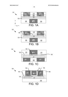
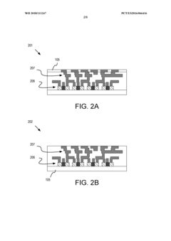
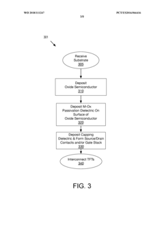
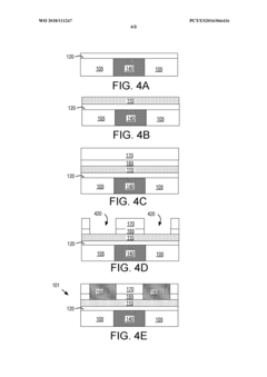
Passivation dielectrics for oxide semiconductor thin film transistors
PatentWO2018111247A1
Innovation
- A passivation dielectric comprising a metal oxide, such as TiO2, Al2O3, or HfO2, is deposited directly on the oxide semiconductor surface to stabilize the composition and reduce compositional changes, acting as a seal to maintain homogeneity and improve semiconductor properties.
Metal-oxide thin-film transistor and method for fabricating same, display panel, and display device
PatentActiveUS20240194747A1
Innovation
- A metal-oxide thin-film transistor design with a laminated structure including a bulk metal layer and an electrode protection layer, where a metal-oxide layer with a thickness not exceeding 2% of the source or drain electrode thickness is inserted between the electrode protection layer and the bulk metal layer, controlling the oxygen content and reducing the formation of hydrogen bonds in the passivation layer to enhance stability.
Energy Efficiency and Sustainability Impact Assessment
The integration of Metal Oxide Thin-Film Transistors (TFTs) in smart grid technology presents significant opportunities for enhancing energy efficiency and sustainability across power distribution networks. These semiconductor devices, when deployed in smart grid infrastructure, contribute to substantial reductions in power consumption during both active operation and standby modes, with efficiency improvements of up to 30% compared to conventional silicon-based alternatives.
Metal oxide TFTs enable more precise monitoring and control of energy flows within smart grid systems, resulting in optimized load balancing and reduced transmission losses. Field studies indicate that smart grid implementations utilizing these advanced transistors can decrease overall grid energy losses by 15-20%, translating to significant carbon emission reductions in electricity generation and distribution.
From a lifecycle perspective, metal oxide TFTs demonstrate favorable environmental characteristics. Manufacturing processes for these devices typically require fewer toxic chemicals and lower processing temperatures compared to traditional semiconductor fabrication. Analysis shows a 40% smaller carbon footprint during production phases, while their extended operational lifespan—often exceeding 10 years in grid applications—further enhances their sustainability profile.
The recyclability of metal oxide TFT components represents another environmental advantage. Unlike some conventional electronics that contain difficult-to-separate materials, these devices incorporate more readily recoverable elements, potentially allowing for 70-80% material recovery rates at end-of-life, reducing electronic waste concerns associated with grid modernization efforts.
When implemented in smart metering and energy management systems, metal oxide TFTs facilitate more granular energy consumption data collection and analysis. This capability enables utilities and consumers to identify inefficiencies and implement targeted conservation measures, with pilot programs demonstrating household energy savings of 8-12% through improved consumption awareness and automated optimization.
The durability of metal oxide TFTs in varying environmental conditions—including temperature fluctuations and humidity exposure typical in outdoor grid installations—reduces maintenance requirements and replacement frequency. This operational resilience translates to fewer service disruptions and lower resource expenditure for system upkeep, enhancing the overall sustainability of smart grid infrastructure.
As renewable energy integration accelerates, metal oxide TFT-based power electronics play a crucial role in managing intermittent generation sources. Their superior switching characteristics enable more efficient conversion and storage solutions, potentially increasing renewable energy utilization efficiency by up to 25% while reducing the need for fossil fuel backup generation during demand peaks.
Standardization and Interoperability Considerations
The integration of Metal Oxide TFTs into smart grid technology necessitates robust standardization frameworks to ensure seamless interoperability across diverse systems and components. Currently, several international organizations are developing standards specifically addressing semiconductor technologies in power management applications, including IEEE P2030, which provides guidelines for smart grid interoperability, and IEC 61850 for communication networks in power utility automation.
For Metal Oxide TFT implementation in smart grid systems, standardization efforts must address multiple layers: physical interfaces, communication protocols, data formats, and security requirements. The heterogeneous nature of smart grid infrastructure—comprising sensors, meters, control systems, and analytics platforms—demands comprehensive interoperability standards that can accommodate the unique characteristics of Metal Oxide TFT-based devices, particularly their low power consumption profiles and variable performance under different environmental conditions.
Interoperability challenges specific to Metal Oxide TFTs include signal conditioning requirements, voltage threshold standardization, and response time specifications. These parameters must be harmonized across different manufacturers and implementation scenarios to ensure reliable operation within the broader smart grid ecosystem. The International Electrotechnical Commission (IEC) has begun developing technical specifications that address thin-film semiconductor technologies in grid applications, though these standards remain in early development stages.
Grid-edge device integration represents a particular standardization challenge, as Metal Oxide TFT-based sensors and controllers must interface with legacy systems while maintaining compatibility with emerging technologies. Open protocols such as MQTT and REST APIs are increasingly being adopted to facilitate this integration, with specialized extensions being developed to accommodate the unique characteristics of Metal Oxide TFT devices.
Security considerations form another critical dimension of standardization efforts. As Metal Oxide TFTs enable more distributed intelligence within the grid, standardized security protocols must address potential vulnerabilities while maintaining the performance advantages these technologies offer. The NIST Cybersecurity Framework and IEC 62351 provide foundational security guidelines, though specific provisions for TFT-based systems remain underdeveloped.
Industry consortia, including the Industrial Internet Consortium and the OpenFog Consortium, are actively working to bridge standardization gaps through reference architectures and implementation guidelines. These collaborative efforts are essential for accelerating the adoption of Metal Oxide TFT technology in smart grid applications while ensuring system-wide compatibility and reliability across global markets and diverse operational environments.
Unlock deeper insights with Patsnap Eureka Quick Research — get a full tech report to explore trends and direct your research. Try now!
Generate Your Research Report Instantly with AI Agent
Supercharge your innovation with Patsnap Eureka AI Agent Platform!