Metal Oxide TFT and Polymer Compatibility in Next-Gen Devices
SEP 28, 20259 MIN READ
Generate Your Research Report Instantly with AI Agent
Patsnap Eureka helps you evaluate technical feasibility & market potential.
Metal Oxide TFT Evolution and Objectives
Metal oxide thin-film transistors (TFTs) have undergone remarkable evolution since their inception in the early 2000s. Initially developed as an alternative to amorphous silicon (a-Si) and polycrystalline silicon (poly-Si) technologies, metal oxide semiconductors, particularly those based on indium gallium zinc oxide (IGZO), emerged as promising candidates for next-generation display technologies. The fundamental advantage of these materials lies in their unique electronic structure, where the conduction band is primarily composed of spherically symmetric metal s-orbitals, enabling high electron mobility even in amorphous states.
The technological trajectory of metal oxide TFTs has been characterized by continuous improvements in performance metrics. Early iterations demonstrated electron mobilities of 5-10 cm²/Vs, which have now been enhanced to exceed 50 cm²/Vs in optimized structures. This progression has been accompanied by significant reductions in operating voltage, enhanced stability under bias stress conditions, and improved uniformity across large-area substrates.
A pivotal milestone in metal oxide TFT development was the transition from rigid glass substrates to flexible platforms. This shift necessitated the development of low-temperature deposition processes, as conventional high-temperature annealing (>300°C) was incompatible with polymer substrates. Solution-processing methods, including sol-gel techniques and combustion synthesis, have emerged as viable alternatives to vacuum-based deposition, offering cost advantages and compatibility with roll-to-roll manufacturing.
The integration of metal oxide TFTs with polymer substrates represents a critical technological objective for enabling truly flexible and conformable electronic devices. This integration faces several challenges, including thermal budget limitations, mechanical stress at the interface, and chemical compatibility between inorganic semiconductors and organic polymers. The development of effective barrier layers and interface engineering strategies has become essential to mitigate these issues.
Current research objectives focus on achieving seamless compatibility between metal oxide TFTs and polymer substrates while maintaining high performance and reliability. This includes developing low-temperature processing techniques that preserve the intrinsic advantages of metal oxide semiconductors, designing flexible encapsulation solutions to protect against environmental degradation, and creating robust interfaces that can withstand repeated mechanical deformation.
The ultimate goal is to establish a technological foundation for next-generation flexible displays, wearable electronics, and conformable sensors that combine the high performance of metal oxide semiconductors with the mechanical flexibility and lightweight properties of polymers. This convergence is expected to enable novel form factors and applications that transcend the limitations of conventional rigid electronics, opening new frontiers in human-machine interfaces and ubiquitous computing environments.
Market Analysis for Next-Gen Display Technologies
The display technology market is experiencing a significant transformation driven by the integration of Metal Oxide Thin-Film Transistors (TFTs) and polymer materials in next-generation devices. Current market projections indicate that the global display market will reach approximately 169 billion USD by 2025, with flexible and foldable displays representing the fastest-growing segment at a compound annual growth rate of 35%.
Metal oxide TFT-based displays, particularly those utilizing Indium Gallium Zinc Oxide (IGZO) and Zinc Oxide (ZnO) technologies, have captured substantial market share in premium consumer electronics. These technologies currently account for roughly 27% of the high-end smartphone display market and 18% of the tablet display market, with continued growth expected as manufacturing costs decrease.
The compatibility between metal oxide TFTs and polymer substrates has created new market opportunities in wearable technology, automotive displays, and healthcare monitoring devices. Market research indicates that the wearable display segment alone is projected to grow by 42% annually through 2026, largely driven by advancements in flexible display technologies that combine these materials.
Consumer demand patterns show increasing preference for devices with higher resolution, lower power consumption, and enhanced form factors—all benefits offered by metal oxide TFT technology when paired with polymer substrates. This trend is particularly evident in the Asia-Pacific region, where 65% of global display manufacturing capacity is concentrated, with South Korea, Japan, and Taiwan leading innovation in this space.
Industry analysts have identified several key market drivers for metal oxide TFT and polymer compatibility technologies: the growing demand for foldable smartphones (projected 50% year-over-year growth), increasing adoption of OLED displays in various applications, and the expansion of the Internet of Things (IoT) ecosystem requiring flexible, low-power displays.
Competitive landscape analysis reveals that major display manufacturers including Samsung Display, LG Display, BOE Technology, and Japan Display Inc. have made substantial investments in metal oxide TFT research and production facilities. Samsung alone has allocated over 13 billion USD toward next-generation display technologies over the past five years, with specific focus on metal oxide semiconductor integration with polymer substrates.
Market barriers include high initial manufacturing costs, yield challenges when scaling production, and competition from alternative technologies such as Low-Temperature Polysilicon (LTPS). However, the superior electron mobility and stability of metal oxide TFTs, combined with the flexibility and durability of advanced polymers, position this technology combination favorably for long-term market growth across multiple industry verticals.
Technical Barriers in Metal Oxide-Polymer Integration
The integration of metal oxide thin-film transistors (TFTs) with polymer substrates presents significant technical challenges despite its promising applications in flexible electronics. One primary barrier is the inherent thermal incompatibility between these materials. Metal oxide semiconductors typically require high-temperature processing (>300°C) for optimal performance, while most flexible polymers degrade at temperatures above 150-200°C. This fundamental mismatch necessitates the development of low-temperature deposition techniques that maintain semiconductor quality without compromising substrate integrity.
Interface adhesion issues represent another critical barrier. Metal oxides and polymers exhibit vastly different surface energies and chemical properties, often resulting in poor adhesion and delamination during device fabrication or operation. This incompatibility is exacerbated by the significant coefficient of thermal expansion (CTE) mismatch between rigid metal oxides and flexible polymers, creating internal stresses that can lead to cracking and device failure during thermal cycling or mechanical deformation.
Chemical stability concerns further complicate integration efforts. Many polymers release organic contaminants during processing that can diffuse into the metal oxide layer, degrading semiconductor performance. Conversely, the precursors and solvents used in metal oxide deposition can attack polymer substrates, causing swelling, dissolution, or chemical degradation that compromises structural integrity.
Mechanical flexibility requirements introduce additional challenges. While polymers offer excellent flexibility, metal oxide films typically exhibit brittle behavior. When deposited on flexible substrates, these films experience strain during bending that can lead to crack formation and propagation. This fundamentally limits the minimum bending radius achievable in flexible devices and reduces operational lifetime under repeated flexing conditions.
Environmental stability represents a significant long-term barrier. Metal oxide-polymer interfaces are particularly vulnerable to moisture and oxygen penetration, which can degrade both materials and their interface. This vulnerability necessitates effective encapsulation strategies that maintain flexibility while providing robust environmental protection.
Manufacturing scalability presents perhaps the most significant commercialization barrier. Current laboratory techniques for low-temperature metal oxide deposition on polymers often involve complex processes with low throughput and yield. Transitioning these methods to high-volume manufacturing while maintaining performance consistency and cost-effectiveness remains challenging. Additionally, the integration of these hybrid structures into complete device architectures requires compatible processing for all layers, further complicating manufacturing workflows.
Current Integration Solutions for Metal Oxide-Polymer Systems
01 Metal oxide TFT fabrication with polymer substrates
Metal oxide thin-film transistors can be fabricated on flexible polymer substrates to create bendable electronic devices. This approach combines the high electron mobility of metal oxide semiconductors with the flexibility of polymer materials. Special processing techniques are required to ensure compatibility between the metal oxide layer and the polymer substrate, including low-temperature deposition methods that prevent substrate damage.- Metal oxide semiconductor materials for TFTs: Various metal oxide semiconductor materials can be used in thin-film transistors (TFTs) to achieve compatibility with polymers. These materials include zinc oxide, indium gallium zinc oxide (IGZO), and other metal oxide combinations that offer high electron mobility and good electrical performance. The selection of appropriate metal oxide materials is crucial for ensuring compatibility with polymer substrates and achieving desired TFT performance characteristics.
- Polymer substrates for flexible TFT applications: Polymer substrates such as polyimide, polyethylene terephthalate (PET), and other flexible polymers can be used as base materials for metal oxide TFTs. These substrates provide flexibility, lightweight properties, and compatibility with various manufacturing processes. The integration of metal oxide semiconductors with polymer substrates enables the development of flexible and bendable electronic devices while maintaining electrical performance.
- Interface engineering between metal oxides and polymers: Interface engineering techniques are employed to improve compatibility between metal oxide semiconductors and polymer materials. These techniques include surface treatments, buffer layers, and adhesion promoters that enhance the interface quality and reduce defects. Proper interface engineering is essential for achieving good electrical contact, reducing charge trapping, and ensuring long-term device stability in metal oxide TFTs with polymer components.
- Low-temperature processing methods for polymer compatibility: Low-temperature processing methods are developed to enable the fabrication of metal oxide TFTs on temperature-sensitive polymer substrates. These methods include solution processing, atomic layer deposition, and other techniques that allow for the deposition and annealing of metal oxide semiconductors at temperatures compatible with polymers. These approaches prevent substrate deformation while ensuring good semiconductor performance.
- Polymer dielectrics and encapsulation for metal oxide TFTs: Polymer materials can be used as dielectric layers and encapsulation in metal oxide TFTs. These polymer dielectrics provide good insulating properties, flexibility, and compatibility with metal oxide semiconductors. Additionally, polymer encapsulation protects the TFT devices from environmental factors such as moisture and oxygen, enhancing device stability and lifetime while maintaining the benefits of both metal oxide semiconductors and polymer materials.
02 Polymer dielectrics for metal oxide TFTs
Polymer materials can serve as gate dielectric layers in metal oxide TFTs, providing advantages such as solution processability and flexibility. The interface between the polymer dielectric and the metal oxide semiconductor is critical for device performance. Specific polymer formulations have been developed that are chemically compatible with metal oxide semiconductors while maintaining excellent insulating properties and stability during operation.Expand Specific Solutions03 Encapsulation of metal oxide TFTs with polymer materials
Polymer encapsulation layers protect metal oxide TFTs from environmental factors such as moisture and oxygen that can degrade device performance. These encapsulation techniques involve applying polymer barriers that are chemically compatible with the metal oxide while providing effective sealing properties. Advanced multilayer structures combining different polymer materials can enhance the protection while maintaining flexibility of the overall device.Expand Specific Solutions04 Interface engineering between metal oxides and polymers
The interface between metal oxide semiconductors and polymer materials is critical for device performance and stability. Various surface treatments and interlayers can be used to improve compatibility and adhesion between these dissimilar materials. Techniques such as plasma treatment, self-assembled monolayers, and gradient composition layers help reduce interface defects and charge trapping, resulting in improved electrical characteristics and device longevity.Expand Specific Solutions05 Solution-processed metal oxide and polymer composite systems
Solution processing techniques enable the integration of metal oxide semiconductors with polymer materials in a cost-effective manner. These methods include sol-gel processes, nanoparticle dispersions, and hybrid organic-inorganic formulations that can be deposited by printing or coating. The resulting composite systems combine the electrical performance of metal oxides with the processing advantages of polymers, enabling large-area, flexible electronic devices with tunable properties.Expand Specific Solutions
Industry Leaders in Metal Oxide TFT Manufacturing
The metal oxide TFT and polymer compatibility market is currently in a growth phase, with increasing adoption in next-generation display technologies. The global market is expanding rapidly, driven by demand for flexible, lightweight, and energy-efficient devices. Leading players like Samsung Electronics, BOE Technology, and TCL China Star Optoelectronics are investing heavily in this technology, while specialized firms such as Flexterra and Cbrite focus on innovative TFT solutions. Research institutions including South China University of Technology and Gwangju Institute of Science & Technology are advancing fundamental technologies. The market shows varying degrees of technical maturity, with metal oxide TFTs (particularly IGZO) reaching commercial viability while polymer compatibility solutions are still evolving, creating opportunities for companies like Semiconductor Energy Laboratory and Applied Materials to develop breakthrough manufacturing processes.
BOE Technology Group Co., Ltd.
Technical Solution: BOE has developed a comprehensive metal oxide TFT solution for flexible displays that focuses on polymer compatibility through their "Oxide 2.0" technology platform. Their approach utilizes a multi-layer architecture where specially formulated buffer layers are deposited between the polymer substrate and the metal oxide semiconductor to manage thermal expansion differences and enhance adhesion. BOE's technology employs a modified IGZO composition with added stabilizing elements that maintain performance at the low processing temperatures (below 150°C) required for polymer substrates. They've pioneered a proprietary "self-aligned" fabrication process that reduces mask steps and minimizes alignment issues that typically occur with flexible substrates. For enhanced polymer compatibility, BOE has developed specialized passivation materials that simultaneously protect the oxide semiconductor from environmental degradation while providing mechanical stress relief during bending. Their solution achieves electron mobility of 15-20 cm²/Vs while maintaining stability under repeated bending cycles (>100,000 cycles at 5mm radius).
Strengths: Large-scale production capability; comprehensive vertical integration from materials to finished displays; strong patent portfolio in flexible display technologies. Weaknesses: Slightly lower electron mobility compared to rigid substrate implementations; requires specialized encapsulation technologies to prevent moisture ingress; higher defect rates in mass production compared to conventional glass-based displays.
Flexterra, Inc.
Technical Solution: Flexterra has developed a revolutionary approach to metal oxide TFT and polymer compatibility through their proprietary "FlexOS" technology platform. Unlike conventional approaches that adapt existing oxide semiconductor processes to polymer substrates, Flexterra has engineered their metal oxide formulations specifically for optimal performance on polymer materials from the ground up. Their solution utilizes a unique soluble metal oxide precursor system that can be solution-processed at temperatures as low as 120°C, well below the thermal limits of most polymer substrates. This approach enables direct patterning through additive manufacturing techniques like inkjet printing, significantly reducing production steps and material waste. Flexterra's technology incorporates specialized interface engineering with self-assembled monolayers that enhance adhesion between the oxide semiconductor and polymer substrate while providing effective moisture barriers. Their metal oxide formulation achieves electron mobility of 8-12 cm²/Vs on polymer substrates while maintaining excellent stability under mechanical strain, with less than 10% performance variation after 100,000 bending cycles at a 3mm radius.
Strengths: Solution-processable technology enabling lower-cost manufacturing; excellent compatibility with a wide range of polymer substrates; environmentally friendly production with reduced waste. Weaknesses: Lower electron mobility compared to vacuum-deposited oxide semiconductors; more sensitive to environmental contaminants during processing; less established in high-volume manufacturing environments.
Key Patents in Metal Oxide TFT-Polymer Compatibility
Stability enhancements in metal oxide semiconductor thin film transistors
PatentWO2010074927A2
Innovation
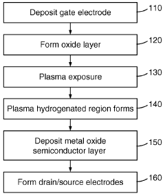
- Exposing the dielectric layer to a hydrogen-containing plasma before depositing the metal oxide semiconductor layer creates a hydrogenated region at the semiconductor-dielectric interface, enhancing carrier mobility and reducing hysteresis, thereby stabilizing the TFTs.
Thin film transistor using an oxide semiconductor and display
PatentInactiveEP2248179A1
Innovation
- A thin film transistor with a channel layer composed of indium (In), germanium (Ge), and oxygen (O) with specific compositional ratios, allowing for amorphous phase formation at room temperature, providing enhanced stability and performance by optimizing the In/(In+Ge) ratio between 0.5 and 0.97, and using a silicon oxide gate insulation layer for improved reliability.
Sustainability Aspects of Metal Oxide TFT Technologies
The sustainability profile of metal oxide TFT technologies represents a critical consideration in their widespread adoption for next-generation devices. These technologies offer significant environmental advantages compared to conventional silicon-based alternatives, primarily due to their lower processing temperatures. While traditional silicon TFTs require high-temperature processing (often exceeding 300°C), metal oxide TFTs can be manufactured at temperatures below 200°C, resulting in substantially reduced energy consumption during production.
Material efficiency constitutes another key sustainability benefit. Metal oxide semiconductors typically utilize abundant elements such as indium, gallium, zinc, and tin, which can be deposited in extremely thin layers (often less than 50nm). This minimal material usage contrasts favorably with the relatively material-intensive silicon-based processes, though concerns regarding indium scarcity remain relevant for certain formulations.
The compatibility of metal oxide TFTs with flexible polymer substrates further enhances their sustainability credentials. This compatibility enables the development of lightweight, flexible devices that require less material overall and can potentially reduce transportation-related carbon emissions. Additionally, the extended lifetime of metal oxide TFTs compared to organic alternatives translates to reduced electronic waste generation over time.
Recycling considerations present both challenges and opportunities. While the thin-film nature of these devices complicates material recovery, research into delamination techniques shows promise for separating valuable metal oxides from polymer substrates. Several research groups have demonstrated recovery rates exceeding 80% for indium from end-of-life devices, suggesting viable recycling pathways.
Water usage during manufacturing represents a sustainability concern, as wet etching processes commonly employed in metal oxide TFT production can consume significant quantities of ultrapure water. However, emerging dry etching techniques and solution-processed metal oxide formulations offer potential pathways to reduce water consumption by up to 40% compared to current manufacturing methods.
From a lifecycle perspective, the lower operating voltages of metal oxide TFTs (typically 1-5V versus 10-15V for amorphous silicon) contribute to energy savings during device operation. When combined with their manufacturing efficiency, these technologies demonstrate favorable cradle-to-grave environmental impacts, with lifecycle assessments indicating potential carbon footprint reductions of 15-30% compared to conventional TFT technologies.
Manufacturing Scalability Challenges and Solutions
The integration of metal oxide TFTs with polymer substrates presents significant manufacturing scalability challenges that must be addressed for commercial viability. Traditional manufacturing processes for metal oxide semiconductors typically require high temperatures (300-500°C), which exceed the thermal tolerance of most polymer substrates that degrade at temperatures above 150-200°C. This fundamental incompatibility has necessitated the development of alternative deposition techniques and process modifications.
Low-temperature deposition methods have emerged as critical enablers for large-scale manufacturing. Solution-processing techniques, including spin-coating, inkjet printing, and spray coating, allow for metal oxide precursor deposition at temperatures compatible with polymer substrates. However, these methods often struggle with uniformity across large areas, presenting yield challenges when scaling to industrial production volumes.
Roll-to-roll (R2R) processing represents a promising approach for high-throughput manufacturing of flexible devices. This continuous production method can significantly reduce per-unit costs compared to batch processing, but requires precise control of tension, alignment, and environmental conditions. Current R2R systems for metal oxide TFT production achieve throughput rates of 5-10 m²/min, though defect densities remain higher than traditional silicon manufacturing.
Interface engineering between metal oxides and polymers presents another significant challenge. Adhesion issues, mechanical stress during flexing, and chemical incompatibilities can lead to delamination and device failure. Industrial solutions include the development of specialized adhesion layers and surface treatments that can be applied at scale without compromising electrical performance.
Encapsulation technologies have proven essential for device longevity but add complexity to the manufacturing process. Atomic Layer Deposition (ALD) provides excellent barrier properties but faces throughput limitations in high-volume production. Alternative multi-layer barrier films offer a more scalable solution, though with some compromise in performance.
Equipment standardization remains underdeveloped, with many manufacturers using customized tools rather than standardized platforms. This fragmentation increases costs and limits knowledge transfer across the industry. Recent consortium efforts are working to establish common equipment specifications and process parameters to accelerate industrial adoption.
Yield management systems specifically designed for flexible electronics manufacturing are still in their infancy. Unlike silicon manufacturing with decades of established statistical process control methods, metal oxide TFT production on polymers lacks robust in-line monitoring techniques capable of detecting defects in high-speed production environments without damaging sensitive substrates.
Unlock deeper insights with Patsnap Eureka Quick Research — get a full tech report to explore trends and direct your research. Try now!
Generate Your Research Report Instantly with AI Agent
Supercharge your innovation with Patsnap Eureka AI Agent Platform!