Metal Oxide TFT Applications in Advanced Data Storage Solutions
SEP 28, 20259 MIN READ
Generate Your Research Report Instantly with AI Agent
Patsnap Eureka helps you evaluate technical feasibility & market potential.
Metal Oxide TFT Evolution and Objectives
Metal oxide thin-film transistors (TFTs) have undergone remarkable evolution since their inception in the early 2000s. Initially developed as an alternative to amorphous silicon (a-Si) and polycrystalline silicon (poly-Si) TFTs, metal oxide semiconductors, particularly those based on indium gallium zinc oxide (IGZO), have demonstrated superior electrical properties including higher electron mobility, better uniformity, and enhanced stability. The journey began with the pioneering work of Hosono and colleagues at the Tokyo Institute of Technology, who first demonstrated the potential of transparent amorphous oxide semiconductors in 2004.
The evolution of metal oxide TFTs has been characterized by continuous improvements in material composition, deposition techniques, and device architectures. Early iterations faced challenges related to stability, particularly under bias stress conditions, and manufacturing scalability. However, subsequent research focused on optimizing the oxygen vacancy concentration, controlling impurities, and developing novel passivation techniques has significantly enhanced device performance and reliability.
From 2010 to 2015, the field witnessed substantial progress in low-temperature processing techniques, enabling compatibility with flexible substrates and expanding potential applications beyond traditional rigid electronics. The development of solution-processed metal oxide TFTs further democratized the technology by offering cost-effective manufacturing alternatives to vacuum-based deposition methods.
Recent advancements have focused on enhancing carrier mobility, which has improved from less than 10 cm²/Vs in early devices to exceeding 50 cm²/Vs in optimized structures. This improvement has been achieved through careful engineering of material interfaces, development of multi-component oxide systems, and implementation of novel doping strategies.
In the context of advanced data storage solutions, metal oxide TFTs aim to address several critical objectives. Primarily, they seek to enable higher-density storage arrays by providing superior switching characteristics and reduced pixel sizes compared to conventional silicon-based technologies. The excellent uniformity of metal oxide TFTs facilitates precise control of threshold voltages across large arrays, which is essential for reliable multi-level cell operations in memory applications.
Another key objective is to support the development of three-dimensional (3D) storage architectures, where metal oxide TFTs can serve as vertical access devices due to their excellent scalability and low leakage currents. Additionally, these devices target reduced power consumption in storage systems through lower operating voltages and improved subthreshold swing characteristics.
The technology also aims to enhance the integration of sensing and memory functions, potentially enabling in-memory computing paradigms that could revolutionize data processing architectures. Looking forward, metal oxide TFTs are positioned to play a crucial role in emerging neuromorphic computing systems, where their analog switching behavior can emulate synaptic functions.
Market Analysis for Advanced Data Storage Solutions
The global advanced data storage market is experiencing unprecedented growth, driven by the explosion of data generation across industries. Current market valuations place the advanced storage solutions sector at approximately $56 billion, with projections indicating a compound annual growth rate of 16.5% through 2028. This remarkable expansion is primarily fueled by the increasing adoption of cloud computing services, big data analytics, and the proliferation of IoT devices generating massive data volumes requiring efficient storage solutions.
Metal oxide thin-film transistor (TFT) technology is emerging as a disruptive force in this landscape, offering significant advantages over conventional silicon-based storage architectures. Market research indicates that metal oxide TFT-based storage solutions could capture up to 12% of the advanced storage market within the next five years, representing a substantial opportunity for early adopters and innovators in this space.
Demand segmentation reveals particularly strong growth potential in enterprise data centers, which currently account for 43% of advanced storage solution deployments. These facilities are increasingly seeking higher density storage with reduced power consumption – precisely the benefits that metal oxide TFT technology promises to deliver. Healthcare and financial services verticals demonstrate the highest adoption rates, with 27% and 22% year-over-year growth respectively in implementing next-generation storage technologies.
Regional analysis shows Asia-Pacific leading the market adoption curve, commanding 38% of global advanced storage solution implementations. This is largely attributed to the concentration of semiconductor manufacturing capabilities and aggressive digital transformation initiatives across the region. North America follows closely at 32%, with particularly strong demand from cloud service providers and data-intensive industries.
Customer surveys reveal five critical purchasing factors driving market demand: storage density (cited by 87% of respondents), power efficiency (82%), reliability (79%), cost-effectiveness (76%), and integration capabilities (68%). Metal oxide TFT technology demonstrates competitive advantages in four of these five categories, positioning it favorably against alternative emerging storage technologies.
Pricing trends indicate a steady decline in cost-per-terabyte for advanced storage solutions, with metal oxide TFT implementations potentially accelerating this trend through simplified manufacturing processes and reduced material costs. Industry analysts project that metal oxide TFT storage solutions could achieve cost parity with conventional technologies by 2025, after which they may establish a significant price advantage.
Technical Challenges in Metal Oxide TFT Implementation
Despite the promising potential of metal oxide thin-film transistors (TFTs) in advanced data storage solutions, several significant technical challenges impede their widespread implementation. The primary obstacle lies in achieving consistent electrical performance across large-area substrates. Metal oxide TFTs, particularly those based on indium-gallium-zinc oxide (IGZO), exhibit spatial variations in threshold voltage and mobility, which can lead to inconsistent operation in storage array applications where uniformity is paramount.
Material stability presents another critical challenge, as metal oxide semiconductors can be sensitive to environmental factors. Exposure to humidity, oxygen, and light can alter the electrical characteristics of these devices over time, potentially compromising data integrity in storage applications. This necessitates robust encapsulation technologies and passivation layers that add complexity to the fabrication process.
Interface engineering remains problematic, particularly at the semiconductor-dielectric interface where charge trapping phenomena can occur. These trapped charges contribute to threshold voltage shifts and hysteresis effects, which are detrimental to reliable data storage operations. The development of high-quality dielectric materials with minimal interface states continues to be an active area of research.
Scaling limitations also pose significant hurdles. As storage densities increase, metal oxide TFTs must be scaled down accordingly. However, short-channel effects become pronounced at reduced dimensions, leading to degraded switching characteristics and increased leakage currents. This fundamentally limits the storage density achievable with current metal oxide TFT technologies.
Process integration challenges arise when incorporating metal oxide TFTs into existing semiconductor manufacturing flows. The temperature sensitivity of many metal oxide materials restricts the thermal budget available for subsequent processing steps. Additionally, compatibility issues with common semiconductor materials and processes can complicate integration efforts.
Contact resistance at the source/drain interfaces represents another technical barrier. High contact resistance limits current drive capability and switching speed, both critical parameters for high-performance data storage applications. Developing low-resistance ohmic contacts to metal oxide semiconductors without degrading the semiconductor properties remains challenging.
Bias stress instability further complicates implementation, as prolonged voltage application can cause threshold voltage shifts due to charge trapping or defect creation. This instability is particularly problematic for data storage applications requiring long-term reliability and consistent performance over thousands of read/write cycles.
Finally, radiation hardness concerns emerge in certain applications where data integrity must be maintained in harsh environments. Metal oxide TFTs can exhibit sensitivity to ionizing radiation, potentially leading to parameter shifts or even functional failure in radiation-exposed environments.
Current Metal Oxide TFT Storage Solutions
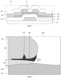
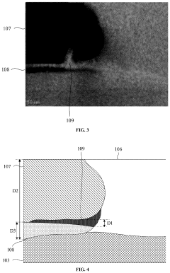
01 Metal oxide semiconductor materials for TFTs
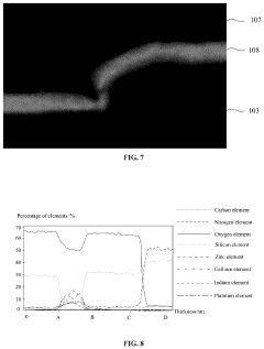
Various metal oxide semiconductor materials can be used in thin-film transistors (TFTs) to achieve specific electrical properties. These materials include indium gallium zinc oxide (IGZO), zinc oxide (ZnO), and other metal oxide combinations that offer advantages such as high electron mobility, good stability, and transparency. The selection of appropriate metal oxide materials is crucial for determining the performance characteristics of the TFT, including switching speed, power consumption, and reliability.- Metal oxide semiconductor materials for TFT fabrication: Various metal oxide semiconductor materials are used in the fabrication of thin-film transistors (TFTs). These materials include indium gallium zinc oxide (IGZO), zinc oxide (ZnO), and other metal oxide combinations that offer advantages such as high electron mobility, good transparency, and stability. The selection of appropriate metal oxide materials is crucial for determining the performance characteristics of the TFT, including switching speed, power consumption, and reliability.
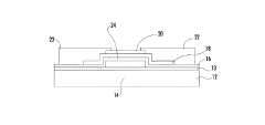
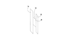
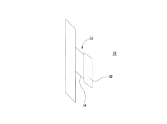
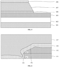
- TFT structure and device architecture: The structural design of metal oxide TFTs significantly impacts their performance. Various architectures such as bottom-gate, top-gate, staggered, and coplanar configurations are employed depending on the application requirements. Each structure offers different advantages in terms of parasitic capacitance, channel control, and integration capability. Advanced structures may incorporate additional features like dual gates, etch stop layers, or specialized contact designs to enhance performance and reliability.
- Fabrication processes and techniques: Specialized fabrication processes are essential for creating high-performance metal oxide TFTs. These include deposition methods such as sputtering, atomic layer deposition (ALD), solution processing, and pulsed laser deposition. Post-deposition treatments like annealing in various atmospheres help optimize the semiconductor properties. Low-temperature processes have been developed to enable fabrication on flexible substrates, while patterning techniques ensure precise device dimensions and integration.
- Integration with display and electronic technologies: Metal oxide TFTs are widely integrated into various display and electronic technologies. They serve as pixel-driving elements in active-matrix displays including LCDs, OLEDs, and emerging display technologies. The integration process involves considerations of interface engineering, passivation layers, and interconnect design. Metal oxide TFTs are also incorporated into sensor arrays, memory devices, and integrated circuits for specialized applications requiring transparent or flexible electronics.
- Performance enhancement and stability improvement: Various approaches are employed to enhance the performance and stability of metal oxide TFTs. These include interface engineering to reduce trap states, doping strategies to control carrier concentration, multilayer channel designs to optimize mobility and stability, and passivation techniques to protect against environmental degradation. Bias stress stability is improved through specialized dielectric materials and treatment processes, while light stability is enhanced through compositional tuning and protective layers.
02 TFT structure and fabrication methods
The structure and fabrication methods of metal oxide TFTs significantly impact their performance. Various configurations such as bottom-gate, top-gate, coplanar, and staggered structures can be employed depending on the application requirements. Fabrication techniques include sputtering, atomic layer deposition, solution processing, and annealing treatments to optimize the metal oxide layer properties. These methods control the crystallinity, defect density, and interface quality of the metal oxide semiconductor layer.Expand Specific Solutions03 Display applications of metal oxide TFTs
Metal oxide TFTs are widely used in display technologies due to their excellent electrical properties and transparency. They serve as switching and driving elements in active-matrix displays including LCDs, OLEDs, and flexible displays. The high electron mobility of metal oxide semiconductors enables faster response times and higher resolution displays, while their transparency allows for increased aperture ratios and improved display brightness.Expand Specific Solutions04 Performance enhancement techniques
Various techniques can be employed to enhance the performance of metal oxide TFTs. These include interface engineering to reduce trap states, doping strategies to control carrier concentration, multi-layer channel structures to optimize electron transport, and passivation layers to improve stability. Additional approaches involve annealing treatments, plasma treatments, and the incorporation of buffer layers to reduce contact resistance and improve overall device performance.Expand Specific Solutions05 Emerging applications and advanced configurations
Metal oxide TFTs are finding applications beyond traditional displays in emerging fields such as sensors, memory devices, and integrated circuits. Advanced configurations include dual-gate structures for enhanced control, complementary TFT circuits combining n-type and p-type devices, and three-dimensional integration for higher density electronics. These developments are enabling new functionalities in flexible electronics, transparent electronics, and large-area electronic systems.Expand Specific Solutions
Industry Leaders in Metal Oxide TFT Technology
The metal oxide TFT market for advanced data storage is currently in a growth phase, with increasing adoption across memory and storage applications. The competitive landscape features established display manufacturers like BOE Technology, TCL China Star, and Samsung Display leveraging their metal oxide expertise into storage solutions, alongside semiconductor specialists including SMIC, Applied Materials, and Huawei. Academic-industry partnerships are accelerating innovation, with institutions like South China University of Technology and Northwestern University collaborating with industry players. The technology is approaching commercial maturity for certain applications, with companies like Semiconductor Energy Laboratory and IMEC leading in oxide semiconductor integration for memory devices, while newer entrants like Innovaflex are exploring flexible storage solutions based on metal oxide TFT architectures.
BOE Technology Group Co., Ltd.
Technical Solution: BOE has developed advanced metal oxide TFT technologies specifically optimized for next-generation data storage applications. Their approach integrates amorphous IGZO (a-IGZO) TFTs with specialized circuit designs to create high-density, low-power memory arrays suitable for both volatile and non-volatile storage applications. BOE's technology utilizes a unique dual-gate structure that enhances carrier mobility while maintaining low leakage currents, critical for data retention in storage applications. The company has demonstrated functional prototypes of IGZO-based RRAM (Resistive Random Access Memory) that combine the switching TFT with a resistive memory element, achieving data retention times exceeding 10 years while operating at voltages below 5V. BOE has also pioneered the integration of these storage elements with their display technologies, creating "memory-in-pixel" architectures that enable new applications in transparent electronics and IoT devices.
Strengths: Vertical integration capabilities from material development to system implementation; established mass production infrastructure; strong IP portfolio in oxide semiconductor applications. Weaknesses: Technology still primarily focused on display applications rather than dedicated storage solutions; faces competition from established memory manufacturers; scaling challenges at advanced nodes.
Semiconductor Energy Laboratory Co., Ltd.
Technical Solution: Semiconductor Energy Laboratory (SEL) has pioneered oxide semiconductor technology, particularly IGZO (Indium Gallium Zinc Oxide) TFTs for advanced data storage applications. Their proprietary c-axis aligned crystalline IGZO (CAAC-IGZO) technology demonstrates exceptional stability and low off-state current characteristics, enabling persistent storage capabilities. SEL has developed oxide semiconductor-based memory cells that combine TFTs with capacitive elements to create high-density storage solutions with significantly reduced power consumption. Their CAAC-IGZO TFTs exhibit off-state current as low as 10^-24 A/μm, allowing for extremely long data retention periods without refresh operations. SEL has also implemented these technologies in three-dimensional stacked memory architectures, increasing storage density while maintaining the benefits of oxide semiconductor properties.
Strengths: Industry-leading low off-state current enabling ultra-long data retention; excellent stability under various environmental conditions; compatibility with existing manufacturing infrastructure. Weaknesses: Higher production costs compared to conventional silicon-based technologies; limited commercialization outside of display applications; requires specialized manufacturing expertise.
Key Patents in Metal Oxide TFT Data Storage
Metal oxide thin film transistor with excellent temperature stability
PatentInactiveJP2016502278A
Innovation
- Implementing a passivation material with a conduction band at least 0.5 eV higher than the metal oxide semiconductor's conduction band to transfer electrons away from the interface, reducing oxygen loss and improving stability by selecting materials like Ta2O5, TiO2, or other insulating oxides that are less susceptible to reduction.
Metal-oxide thin-film transistor and method for fabricating same, display panel, and display device
PatentActiveUS20240194747A1
Innovation
- A metal-oxide thin-film transistor design with a laminated structure including a bulk metal layer and an electrode protection layer, where a metal-oxide layer with a thickness not exceeding 2% of the source or drain electrode thickness is inserted between the electrode protection layer and the bulk metal layer, controlling the oxygen content and reducing the formation of hydrogen bonds in the passivation layer to enhance stability.
Materials Science Advancements for Metal Oxide TFTs
The evolution of metal oxide thin-film transistors (TFTs) has been significantly influenced by breakthroughs in materials science. Initially dominated by amorphous silicon (a-Si) and polycrystalline silicon (poly-Si), the field has witnessed a paradigm shift with the emergence of metal oxide semiconductors such as indium gallium zinc oxide (IGZO), zinc tin oxide (ZTO), and indium zinc oxide (IZO). These materials offer superior electron mobility, ranging from 10-50 cm²/Vs, substantially outperforming traditional a-Si TFTs which typically achieve only 0.5-1 cm²/Vs.
Recent advancements in atomic layer deposition (ALD) and solution-processing techniques have enabled precise control over film thickness and composition at the nanometer scale. This has resulted in metal oxide TFTs with enhanced uniformity and reduced defect density, critical factors for high-density data storage applications. The development of ultra-thin dielectric materials with high-k properties has further improved the gate capacitance and reduced operating voltages to sub-2V levels.
Materials engineering has also addressed the historical stability issues of metal oxide semiconductors. Incorporation of passivation layers composed of Al₂O₃ or SiO₂ has significantly reduced threshold voltage shifts under bias stress conditions from >5V to <0.5V after 10,000 seconds of continuous operation. This enhanced stability is particularly valuable for persistent data storage applications where reliability is paramount.
Doping strategies have emerged as another crucial advancement, with elements such as hafnium and titanium being introduced to modify band structures and carrier concentrations. These dopants have enabled the creation of both n-type and p-type metal oxide semiconductors, facilitating complementary circuit designs that were previously unattainable with traditional metal oxide materials.
The development of flexible and transparent metal oxide TFTs represents another significant materials science breakthrough. By utilizing flexible substrates such as polyimide and incorporating indium-free transparent conductors like aluminum-doped zinc oxide (AZO), researchers have created bendable TFTs that maintain performance metrics even after 10,000 bending cycles at radii below 5mm.
Low-temperature processing techniques have expanded the material compatibility of metal oxide TFTs, allowing integration with temperature-sensitive substrates and components. Solution-processed metal oxide semiconductors can now be fabricated at temperatures below 200°C while maintaining electron mobilities above 5 cm²/Vs, opening new possibilities for integration with advanced memory architectures and three-dimensional storage arrays.
Energy Efficiency Considerations in TFT Storage Applications
Energy efficiency has emerged as a critical factor in the development and implementation of Metal Oxide TFT-based data storage solutions. As data centers continue to expand globally, their energy consumption has become a significant environmental and economic concern, accounting for approximately 1-2% of global electricity usage. Metal oxide TFT technology offers promising advantages in this domain due to its inherently low power consumption characteristics compared to traditional silicon-based transistors.
The power efficiency of metal oxide TFTs stems from their unique material properties, particularly the wide bandgap semiconductors like IGZO (Indium Gallium Zinc Oxide) that enable lower leakage currents during off-states. Recent studies indicate that IGZO-based storage arrays can achieve standby power reductions of up to 70% compared to conventional CMOS technologies, making them particularly suitable for applications requiring frequent transitions between active and idle states.
Thermal management represents another crucial aspect of energy efficiency in TFT storage applications. Metal oxide TFTs generate significantly less heat during operation, reducing cooling requirements in data storage environments. This characteristic translates to cascading energy savings throughout the entire storage infrastructure, as cooling systems typically account for 30-40% of data center energy consumption.
Dynamic power scaling capabilities of metal oxide TFTs further enhance their energy efficiency profile. These devices can operate effectively across a wider voltage range than silicon alternatives, allowing for more granular power management strategies. Advanced power gating techniques specifically designed for metal oxide TFT arrays have demonstrated the ability to reduce active power consumption by up to 45% during low-demand periods without compromising data integrity or access speeds.
Manufacturing considerations also play a vital role in the overall energy footprint of TFT storage solutions. The lower processing temperatures required for metal oxide TFT fabrication (typically below 350°C compared to >1000°C for silicon) result in reduced embodied energy in the final products. Life cycle assessments suggest that this manufacturing advantage can reduce the carbon footprint of storage hardware by approximately 25-30% over traditional technologies.
Integration with renewable energy systems represents an emerging opportunity for metal oxide TFT storage applications. The lower and more consistent power requirements of these systems make them particularly compatible with variable renewable energy sources. Several pilot implementations have demonstrated successful operation of metal oxide TFT storage arrays powered directly by on-site solar generation, highlighting their potential role in sustainable data infrastructure development.
Unlock deeper insights with Patsnap Eureka Quick Research — get a full tech report to explore trends and direct your research. Try now!
Generate Your Research Report Instantly with AI Agent
Supercharge your innovation with Patsnap Eureka AI Agent Platform!