Why Are Metal Oxide TFTs Chosen for High-Speed Computing?
SEP 28, 20259 MIN READ
Generate Your Research Report Instantly with AI Agent
Patsnap Eureka helps you evaluate technical feasibility & market potential.
Metal Oxide TFT Evolution and Computing Objectives
Metal oxide thin-film transistors (TFTs) have evolved significantly since their inception in the early 2000s, transforming from experimental devices to critical components in advanced computing architectures. The journey began with amorphous silicon (a-Si) TFTs dominating display technologies, but their limited electron mobility presented insurmountable barriers for high-speed applications. The breakthrough came with the discovery of amorphous oxide semiconductors, particularly indium gallium zinc oxide (IGZO), which demonstrated electron mobility 10-50 times higher than a-Si while maintaining excellent uniformity across large areas.
The evolution of metal oxide TFTs has been characterized by continuous improvements in material composition, deposition techniques, and device architectures. Early iterations focused primarily on display applications, but researchers quickly recognized their potential for computing tasks. By 2010, metal oxide TFTs had achieved mobility values exceeding 10 cm²/Vs, a critical threshold for integration into computational circuits. The subsequent decade witnessed further refinements in channel materials, introducing elements like hafnium and titanium to enhance performance characteristics.
A pivotal development occurred with the transition from amorphous to crystalline or semi-crystalline structures, which dramatically improved carrier transport properties while maintaining reasonable manufacturing costs. This structural evolution enabled metal oxide TFTs to approach performance levels previously exclusive to conventional silicon-based transistors in certain applications, particularly those requiring moderate computing power with minimal energy consumption.
The computing objectives driving metal oxide TFT development have evolved in parallel with broader industry trends toward edge computing, Internet of Things (IoT), and artificial intelligence applications. These technologies demand processing capabilities in unconventional form factors and environments where traditional silicon CMOS faces fundamental limitations. Metal oxide TFTs offer a compelling solution by enabling computation on flexible, transparent, or large-area substrates, opening new paradigms for human-machine interfaces and ubiquitous computing.
Current research objectives focus on achieving sub-nanosecond switching speeds, reducing operating voltages below 1V, and enhancing long-term stability under various environmental conditions. These goals align with the requirements for neuromorphic computing architectures, where metal oxide TFTs show particular promise due to their tunable conductance states and compatibility with memory elements. The ultimate objective is to develop metal oxide TFT-based computing systems that complement silicon CMOS in specialized applications rather than directly competing with it, creating a heterogeneous computing ecosystem that leverages the unique advantages of each technology.
Market Demand Analysis for High-Speed Computing Solutions
The high-speed computing market has witnessed unprecedented growth in recent years, driven primarily by the increasing demand for faster data processing capabilities across various industries. The global high-performance computing market size was valued at $39.1 billion in 2021 and is projected to reach $65.3 billion by 2026, growing at a CAGR of 10.8%. This substantial growth underscores the critical need for innovative computing solutions that can deliver enhanced performance while maintaining energy efficiency.
Metal oxide thin-film transistors (TFTs) have emerged as a promising technology in this landscape, particularly due to their potential to address several key market demands. The semiconductor industry has been actively seeking alternatives to traditional silicon-based technologies as Moore's Law approaches its physical limits. Metal oxide TFTs offer a viable pathway to continue performance scaling without the prohibitive costs associated with advanced silicon nodes.
Enterprise data centers represent one of the largest market segments driving demand for high-speed computing solutions. With the exponential growth in data generation—estimated at 2.5 quintillion bytes daily—organizations require computing architectures that can process this information efficiently. Metal oxide TFTs, with their superior electron mobility compared to amorphous silicon, can enable faster switching speeds necessary for these data-intensive applications.
The artificial intelligence and machine learning sector has become another significant market driver. The global AI market is expected to grow from $93.5 billion in 2021 to $997.8 billion by 2028. These applications demand massive parallel processing capabilities that traditional computing architectures struggle to deliver efficiently. Metal oxide TFTs offer potential advantages in creating dense, high-performance neural network accelerators due to their favorable power-performance characteristics.
Edge computing represents an emerging market segment with substantial growth potential. As IoT device deployments continue to expand—projected to reach 75.4 billion connected devices by 2025—the need for high-speed, energy-efficient computing at the network edge becomes increasingly critical. Metal oxide TFTs can potentially enable powerful computing capabilities in compact form factors with lower power requirements than conventional technologies.
Consumer electronics manufacturers are also driving demand for advanced computing solutions that can deliver enhanced user experiences while maintaining reasonable battery life. The global consumer electronics market, valued at $1 trillion in 2021, continues to push for devices with greater computational capabilities. Metal oxide TFTs offer a promising path to meeting these requirements through their combination of performance and energy efficiency.
Current State and Challenges of Metal Oxide TFT Technology
Metal oxide thin-film transistors (TFTs) have emerged as a promising technology for high-speed computing applications, yet their current state of development presents both significant achievements and considerable challenges. Globally, metal oxide TFT technology has advanced rapidly over the past decade, with research centers in Asia, particularly in South Korea, Japan, and Taiwan, leading commercial development. European and North American institutions maintain strong positions in fundamental research and novel applications.
The current performance metrics of metal oxide TFTs show impressive characteristics, including electron mobilities typically ranging from 10-50 cm²/Vs, which significantly outperforms amorphous silicon (a-Si) TFTs (0.5-1 cm²/Vs). This higher mobility enables faster switching speeds essential for computing applications. Additionally, these devices demonstrate excellent uniformity across large areas, with variations in threshold voltage typically below 0.2V across 300mm substrates.
Despite these advantages, several technical challenges impede wider adoption in high-speed computing. The most significant limitation remains the relatively low mobility compared to crystalline silicon MOSFETs, which can achieve mobilities exceeding 1000 cm²/Vs. This mobility gap restricts the ultimate switching speed and computational density achievable with metal oxide TFTs.
Stability issues also present major hurdles, particularly under bias stress conditions. Prolonged operation can lead to threshold voltage shifts of several volts, compromising circuit reliability. Environmental sensitivity, especially to humidity and oxygen, necessitates robust encapsulation solutions that add complexity to manufacturing processes.
Channel material optimization remains an active research area, with various compositions of indium-gallium-zinc-oxide (IGZO) and other metal oxide systems being explored to balance mobility, stability, and manufacturability. The industry has yet to converge on a standardized material composition that optimally addresses all requirements for high-speed computing applications.
Manufacturing scalability presents another challenge. While metal oxide TFTs can be fabricated at relatively low temperatures (typically below 350°C), integration with high-performance computing architectures requires addressing interface quality issues and developing compatible process flows that don't compromise the performance of either technology.
Contact resistance at source/drain interfaces often limits device performance, with typical values ranging from 10⁴ to 10⁵ Ω·cm, significantly higher than in conventional silicon technology. This parasitic resistance becomes increasingly problematic as device dimensions shrink for higher integration densities required in computing applications.
The development of complementary logic remains particularly challenging, as most metal oxide TFTs exhibit n-type behavior, while stable and high-performance p-type metal oxide semiconductors have proven difficult to develop. This imbalance complicates the design of energy-efficient computing circuits that traditionally rely on complementary logic architectures.
Current Metal Oxide TFT Implementations for Computing
01 Material composition for high-speed metal oxide TFTs
The choice of metal oxide materials significantly impacts the speed of thin-film transistors. Specific compositions such as indium-gallium-zinc oxide (IGZO), zinc tin oxide (ZTO), and other multi-component metal oxides demonstrate enhanced electron mobility and switching speeds. The incorporation of dopants and careful control of oxygen vacancies in these materials can further optimize carrier transport properties, resulting in faster TFT operation while maintaining stability.- Material selection for high-speed metal oxide TFTs: The choice of metal oxide materials significantly impacts the speed of thin-film transistors. Certain metal oxides like IGZO (Indium Gallium Zinc Oxide) and ZnO-based compounds demonstrate superior electron mobility compared to conventional amorphous silicon, enabling faster switching speeds. The composition and stoichiometry of these materials can be optimized to enhance carrier mobility and improve device performance. Advanced deposition techniques ensure high-quality metal oxide films with minimal defects, which is crucial for maintaining high-speed operation.
- Device structure optimization for enhanced speed: The structural design of metal oxide TFTs plays a critical role in determining their operating speed. Bottom-gate or top-gate configurations with optimized channel lengths and widths can significantly reduce parasitic capacitance and resistance. Implementing multi-channel architectures and advanced gate dielectric materials improves the interface quality between layers, enhancing carrier transport efficiency. Novel device geometries such as vertical channel structures or fin-based designs can further boost performance by maximizing the effective channel width while minimizing footprint.
- Fabrication processes for high-performance TFTs: Advanced fabrication techniques are essential for producing high-speed metal oxide TFTs. Low-temperature processes enable the use of flexible substrates without compromising device performance. Precise control of annealing conditions helps optimize the crystallinity of the metal oxide layer, directly affecting carrier mobility. Solution-based deposition methods offer cost-effective alternatives to vacuum-based techniques while maintaining high performance. Post-deposition treatments such as plasma exposure or passivation layers can reduce defect density and improve stability of high-speed operation.
- Circuit design for maximizing TFT speed: Innovative circuit designs can maximize the inherent speed capabilities of metal oxide TFTs. Implementing complementary logic architectures reduces power consumption while maintaining high switching speeds. Compensation circuits can mitigate the effects of threshold voltage shifts that occur during operation, ensuring consistent high-speed performance. Advanced driving schemes optimize the charging and discharging of parasitic capacitances, reducing delay times. Integration with other semiconductor technologies creates hybrid circuits that leverage the advantages of different materials for optimal speed performance.
- Doping and interface engineering techniques: Controlled doping of metal oxide semiconductors can significantly enhance carrier concentration and mobility, directly improving TFT speed. Interface engineering between the semiconductor and dielectric layers reduces trap states and scattering centers that impede carrier transport. Introducing specific elements or compounds as dopants can modify the band structure of the metal oxide, optimizing it for high-speed applications. Gradient doping profiles create electric field distributions that accelerate carrier movement through the channel. Surface treatments before and after deposition minimize defects at critical interfaces, ensuring fast and reliable device operation.
02 Structural design optimization for speed enhancement
The physical structure of metal oxide TFTs can be engineered to improve operational speed. This includes optimizing channel length/width ratios, implementing multi-gate structures, and developing vertical channel architectures. Advanced gate configurations and strategic placement of source/drain electrodes reduce parasitic capacitance and resistance, leading to improved frequency response and switching speeds. Novel stacking structures also contribute to enhanced carrier mobility pathways.Expand Specific Solutions03 Interface engineering for improved carrier transport
The quality of interfaces between different layers in metal oxide TFTs critically affects device speed. Techniques such as interface passivation, insertion of buffer layers, and surface treatment methods reduce trap states and scattering centers at boundaries. Controlling the semiconductor-dielectric interface properties minimizes carrier trapping and detrapping delays, resulting in faster response times and improved frequency performance in high-speed applications.Expand Specific Solutions04 Advanced fabrication techniques for high-performance TFTs
Novel fabrication methods significantly impact the speed characteristics of metal oxide TFTs. These include low-temperature processing techniques, atomic layer deposition, solution-based methods, and specialized annealing processes. Precise control over film thickness, composition uniformity, and crystallinity during manufacturing leads to enhanced carrier mobility and reduced defect density, directly contributing to faster TFT operation and improved stability under high-frequency conditions.Expand Specific Solutions05 Circuit design and integration strategies for high-speed applications
Integration approaches and circuit design techniques optimize the speed performance of metal oxide TFT-based systems. This includes complementary circuit architectures, novel driving schemes, and specialized layout designs that minimize parasitic effects. Advanced compensation techniques address threshold voltage shifts during high-speed operation, while innovative interconnect strategies reduce signal delays. These approaches enable metal oxide TFTs to achieve the switching speeds required for demanding applications like high-refresh-rate displays and high-frequency logic circuits.Expand Specific Solutions
Key Industry Players in Metal Oxide TFT Development
Metal oxide TFTs are emerging as a preferred technology for high-speed computing applications due to their unique position in the display technology evolution cycle. Currently, the market is transitioning from traditional amorphous silicon to metal oxide semiconductors, with an estimated global market size exceeding $5 billion and growing at 15% annually. Technologically, metal oxide TFTs offer superior electron mobility (10-50 times higher than a-Si), enabling faster switching speeds critical for next-generation computing devices. Companies like BOE Technology, Samsung Electronics, and Sharp have achieved significant breakthroughs in commercializing these technologies, while research institutions such as Semiconductor Energy Laboratory and IMEC are advancing fundamental innovations. Applied Materials and LG Display are developing manufacturing equipment and production processes to scale this technology, positioning metal oxide TFTs at the early mainstream adoption phase of their technological maturity curve.
Applied Materials, Inc.
Technical Solution: Applied Materials has developed comprehensive manufacturing solutions for metal oxide TFT production targeting high-speed computing applications. Their integrated approach encompasses specialized physical vapor deposition (PVD) systems for precise metal oxide semiconductor layer formation with controlled stoichiometry and minimal contamination. Applied Materials' technology enables the deposition of high-quality IGZO films with electron mobility exceeding 15 cm²/Vs through their proprietary rotary target sputtering technology, which ensures uniform composition across large substrate areas. Their process solutions include specialized annealing systems that optimize the metal oxide microstructure while maintaining low thermal budgets compatible with flexible substrates. Applied Materials has also developed advanced etching and passivation technologies specifically designed to preserve the electrical characteristics of metal oxide semiconductors during device fabrication, resulting in TFTs with excellent stability and performance suitable for high-speed computing applications.
Strengths: Comprehensive end-to-end manufacturing solutions; industry-leading process control capabilities; extensive experience in large-area electronics manufacturing; ability to scale technology from R&D to mass production. Weaknesses: Focused primarily on manufacturing equipment rather than device design; dependent on collaboration with device manufacturers for implementation; higher capital investment requirements compared to existing technologies.
Semiconductor Energy Laboratory Co., Ltd.
Technical Solution: Semiconductor Energy Laboratory (SEL) has developed cutting-edge metal oxide TFT technology specifically optimized for high-speed computing applications. Their proprietary C-Axis Aligned Crystal (CAAC) IGZO technology represents a breakthrough in metal oxide semiconductor structure, achieving electron mobility exceeding 20 cm²/Vs while maintaining extremely low off-state current (10^-24 A/μm). SEL's approach features a unique crystalline structure where the c-axes of the IGZO crystals are aligned perpendicular to the substrate surface, significantly reducing grain boundary scattering and enhancing carrier transport. Their manufacturing process incorporates specialized deposition and annealing techniques that create this aligned crystalline structure while maintaining process temperatures below 450°C. SEL has demonstrated functional CPU cores and memory circuits based on their CAAC-IGZO technology, operating at clock frequencies above 5 MHz with power consumption orders of magnitude lower than conventional silicon technologies.
Strengths: Exceptional electron mobility combined with ultra-low off-state current; superior crystalline structure reducing carrier scattering; excellent stability under prolonged operation; compatibility with existing manufacturing infrastructure. Weaknesses: Complex manufacturing process requiring precise control of deposition parameters; higher initial production costs; intellectual property constraints limiting widespread adoption.
Core Technical Advantages of Metal Oxide TFTs
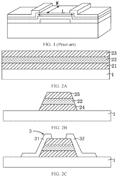
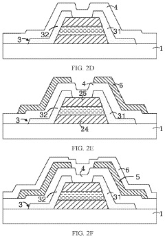
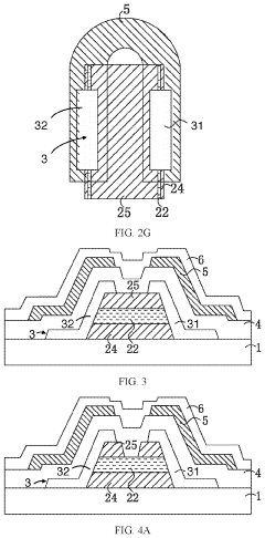
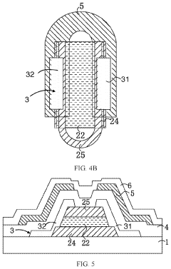
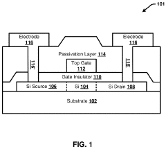
Metal oxide thin-film transistor and manufacturing method for the same
PatentInactiveUS10483405B2
Innovation
- A new metal oxide thin-film transistor structure is developed, where a source electrode and a drain electrode are formed on a substrate with a barrier layer in parallel, and a semiconductor active layer is formed on their side surfaces, allowing for a channel length that is not limited by photolithography precision, enabling a shorter channel design and improved performance.
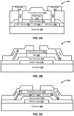
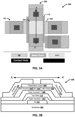
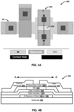
Integration of silicon thin-film transistors and metal-oxide thin film transistors
PatentActiveUS10504939B2
Innovation
- The integration of silicon and metal-oxide TFTs in a 3D stacked configuration, where the metal-oxide TFT is partially stacked over the silicon TFT, sharing gate electrodes or source/drain regions, to create a Metal Oxide on Silicon (MOOS) transistor structure, which reduces pixel area and enables higher pixel densities by combining the benefits of both technologies.
Energy Efficiency Considerations in TFT Computing
Energy efficiency has emerged as a critical factor in the adoption of metal oxide TFTs for high-speed computing applications. The inherent low power consumption characteristics of metal oxide semiconductors, particularly amorphous indium-gallium-zinc oxide (a-IGZO), provide significant advantages in an era where energy constraints increasingly limit computing performance.
Metal oxide TFTs demonstrate remarkably low leakage currents in the off-state, typically in the range of 10^-13 to 10^-12 amperes, which is several orders of magnitude lower than conventional silicon-based transistors. This characteristic substantially reduces static power consumption, which has become increasingly dominant in modern computing systems as device dimensions shrink.
The subthreshold swing of metal oxide TFTs, often below 0.3 V/decade, enables operation at lower supply voltages while maintaining acceptable switching speeds. This voltage scaling directly translates to quadratic reductions in dynamic power consumption, following the power equation P = CV²f, where lower operating voltage (V) significantly reduces overall power requirements.
Thermal management considerations further highlight the energy efficiency advantages of metal oxide TFTs. These devices generate substantially less heat during operation compared to silicon alternatives, reducing cooling requirements and allowing for higher integration densities without thermal throttling. This characteristic is particularly valuable in mobile and edge computing applications where passive cooling is preferred.
The wide bandgap nature of metal oxide semiconductors (typically 3-4 eV) contributes to their energy efficiency by reducing thermally generated carriers and associated leakage currents. This property enables stable operation across broader temperature ranges without significant performance degradation or increased power consumption.
Recent advancements in metal oxide TFT fabrication have yielded devices with mobility values exceeding 10 cm²/Vs while maintaining low threshold voltages. This combination optimizes the energy-delay product, a critical metric for evaluating the energy efficiency of computing elements, allowing for faster computation with minimal energy expenditure.
From a system-level perspective, the compatibility of metal oxide TFTs with large-area, low-temperature processing enables their integration with energy harvesting components and efficient power management circuits. This integration facilitates self-powered or energy-autonomous computing systems for IoT applications, where energy constraints are particularly stringent.
The ability to fabricate metal oxide TFTs on flexible substrates further extends their energy efficiency advantages by enabling conformable, lightweight computing systems that can be powered by smaller batteries or alternative energy sources, opening new frontiers in wearable computing and ubiquitous intelligence.
Manufacturing Scalability and Cost Analysis
The manufacturing scalability of metal oxide TFTs represents a significant advantage driving their adoption in high-speed computing applications. These transistors can be fabricated using existing semiconductor manufacturing infrastructure with relatively minor modifications, allowing for seamless integration into established production lines. This compatibility with current manufacturing processes substantially reduces the capital investment required for mass production, making metal oxide TFTs an economically viable option for large-scale deployment.
From a cost perspective, metal oxide TFTs offer compelling advantages over competing technologies. The raw materials used in their fabrication, primarily metal oxides such as indium gallium zinc oxide (IGZO), are relatively abundant and less expensive than materials required for traditional silicon-based transistors. Additionally, the deposition processes for these materials typically involve lower temperatures, reducing energy consumption during manufacturing and further decreasing production costs.
The simplified device architecture of metal oxide TFTs also contributes to their manufacturing efficiency. With fewer processing steps required compared to conventional silicon transistors, production throughput increases while manufacturing complexity decreases. This streamlined fabrication process translates directly to lower per-unit costs, especially at high production volumes where economies of scale become significant.
Recent advancements in roll-to-roll processing techniques have further enhanced the manufacturing scalability of metal oxide TFTs. This continuous fabrication method enables high-throughput production on flexible substrates, opening new application possibilities while maintaining cost-effectiveness. Industry analyses suggest that as production volumes increase, the cost per transistor for metal oxide TFTs could potentially decrease by 30-40% over the next five years.
The yield rates for metal oxide TFT production have also shown steady improvement, currently reaching 85-90% in optimized manufacturing environments. This high yield further enhances cost efficiency by reducing material waste and rework requirements. As manufacturing processes continue to mature, these yield rates are expected to approach those of conventional silicon technologies, further strengthening the economic case for metal oxide TFTs in high-speed computing applications.
When considering total cost of ownership, metal oxide TFTs demonstrate additional advantages through their lower power consumption requirements, which translate to reduced operational costs over the lifetime of computing devices. This combination of manufacturing scalability, lower material costs, simplified processing, and operational efficiency positions metal oxide TFTs as an increasingly attractive technology for next-generation high-speed computing solutions.
Unlock deeper insights with Patsnap Eureka Quick Research — get a full tech report to explore trends and direct your research. Try now!
Generate Your Research Report Instantly with AI Agent
Supercharge your innovation with Patsnap Eureka AI Agent Platform!