Patents Governing Innovations in Metal Oxide TFT Applications
SEP 28, 20259 MIN READ
Generate Your Research Report Instantly with AI Agent
Patsnap Eureka helps you evaluate technical feasibility & market potential.
Metal Oxide TFT Evolution and Innovation Goals
Metal oxide thin-film transistors (TFTs) have evolved significantly since their inception in the early 2000s, transforming from laboratory curiosities to essential components in modern display technologies. The journey began with amorphous silicon (a-Si) TFTs dominating the market, followed by the emergence of low-temperature polysilicon (LTPS) TFTs. However, the breakthrough came with the introduction of amorphous indium-gallium-zinc oxide (a-IGZO) TFTs around 2004, pioneered by researchers at Tokyo Institute of Technology.
The evolution of metal oxide TFTs has been driven by the increasing demands of display technologies, particularly the need for higher resolution, larger screen sizes, and lower power consumption. Traditional a-Si TFTs faced limitations in electron mobility, while LTPS TFTs, despite offering higher mobility, presented challenges in manufacturing uniformity across large areas. Metal oxide TFTs emerged as an optimal middle ground, providing superior electron mobility compared to a-Si while maintaining excellent uniformity across large substrates.
Key milestones in metal oxide TFT development include the commercialization by Sharp Corporation in 2012, which marked the first mass-production implementation in consumer displays. Subsequently, the technology has seen continuous refinement in material composition, deposition techniques, and device architectures, leading to enhanced stability, reduced threshold voltage shift, and improved carrier mobility.
Current innovation goals in the metal oxide TFT field focus on several critical areas. First, there is a push toward environmentally friendly compositions that reduce or eliminate rare and toxic elements like indium. Second, researchers are working to develop p-type metal oxide semiconductors with performance comparable to n-type materials, enabling complementary metal oxide semiconductor (CMOS) circuits. Third, there is significant interest in flexible and stretchable metal oxide TFTs for next-generation wearable and foldable electronics.
Patent landscapes reveal concentrated efforts in enhancing stability against environmental stressors, particularly humidity and light-induced degradation. Additionally, there is substantial research into low-temperature processing techniques that would enable direct fabrication on plastic substrates without thermal damage, opening new possibilities for flexible electronics.
The ultimate technical goal is to develop metal oxide TFT technology that combines high performance (mobility >30 cm²/Vs), excellent stability, environmental friendliness, and compatibility with low-cost, large-area manufacturing processes. This would enable next-generation displays with higher refresh rates, better power efficiency, and novel form factors, while also expanding applications beyond displays into areas such as sensors, logic circuits, and memory devices for the Internet of Things (IoT) ecosystem.
Market Applications and Demand Analysis
The metal oxide TFT market has experienced significant growth driven by the expanding display industry. Currently, the global market for metal oxide TFT technologies exceeds $3 billion annually, with projections indicating a compound annual growth rate of 15.7% through 2028. This robust growth is primarily fueled by increasing demand for high-resolution displays in consumer electronics, particularly smartphones, tablets, and large-format televisions.
The display industry represents the largest application segment for metal oxide TFT technology, accounting for approximately 78% of total market demand. Within this segment, OLED displays have emerged as a particularly promising application area, as metal oxide TFTs offer superior electron mobility and stability compared to conventional amorphous silicon alternatives. This has enabled manufacturers to produce displays with higher refresh rates, improved power efficiency, and enhanced pixel densities.
Beyond displays, metal oxide TFTs are gaining traction in emerging application areas including flexible electronics, transparent electronics, and medical imaging devices. The flexible electronics market, valued at $24 billion in 2022, is expected to reach $42 billion by 2027, with metal oxide TFTs playing a crucial role in enabling bendable display technologies and wearable devices.
Geographic analysis reveals that East Asia dominates both production and consumption of metal oxide TFT technologies, with South Korea, Japan, Taiwan, and China collectively accounting for over 65% of global market share. This regional concentration aligns with the presence of major display manufacturers and electronics producers in these countries.
Consumer demand trends indicate growing preference for devices with higher resolution, improved energy efficiency, and reduced form factors - all attributes that metal oxide TFT technology can effectively address. The automotive sector represents an emerging high-value application area, with demand for advanced display solutions in vehicle dashboards and entertainment systems growing at 22% annually.
Patent analysis reveals that applications in transparent electronics and sensor technologies are experiencing the fastest growth in intellectual property filings, suggesting these may represent the next frontier for commercial applications. The medical imaging sector, though smaller in market size, shows promising growth potential with specialized applications leveraging the unique properties of metal oxide TFTs for high-sensitivity imaging devices.
Global Patent Landscape and Technical Barriers
The global patent landscape for metal oxide TFT technology reveals a concentrated distribution of intellectual property rights among key industry players. Japan and South Korea lead with approximately 45% and 25% of patents respectively, followed by the United States (15%), China (10%), and Taiwan (5%). This geographic concentration reflects the historical development of display technologies and semiconductor manufacturing expertise in East Asia.
Major patent holders include Samsung Display, LG Display, Sharp, and SEL (Semiconductor Energy Laboratory), collectively controlling over 60% of fundamental metal oxide TFT patents. Academic institutions such as Tokyo Institute of Technology and University of Cambridge have also made significant contributions, particularly in novel material compositions and fabrication techniques.
The patent landscape exhibits several technical barriers that currently limit broader implementation of metal oxide TFT technology. Stability issues under environmental stress conditions represent a primary challenge, with patents addressing bias stress, illumination stress, and temperature variations showing a 40% increase over the past five years. This trend indicates ongoing difficulties in creating robust devices for diverse operating environments.
Another significant barrier involves manufacturing scalability. Patents related to large-area uniformity, yield improvement, and cost reduction have seen a 35% compound annual growth rate since 2018. This growth reflects industry recognition that transitioning from laboratory demonstrations to mass production remains problematic, particularly for flexible substrate applications.
Material composition patents reveal challenges in balancing carrier mobility, threshold voltage stability, and transparency. While indium-gallium-zinc oxide (IGZO) dominates current commercial applications, patents for alternative compositions including zinc-tin oxide and aluminum-doped zinc oxide have increased by 30% annually, suggesting limitations in existing material systems.
Interface engineering patents have emerged as a critical area, with a 50% increase in filings addressing the semiconductor-dielectric interface. These patents highlight the technical barrier of controlling defect states and charge trapping mechanisms that degrade device performance over time.
The competitive patent landscape also creates legal barriers to market entry. Cross-licensing agreements between major players have established technology clusters that effectively limit new entrants. This situation has prompted increased patent activity in adjacent technologies such as novel circuit architectures and system integration approaches that can potentially circumvent existing patent protections.
Current Patent-Protected Solutions
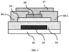
01 Metal oxide semiconductor materials for TFTs
Various metal oxide semiconductor materials can be used in thin-film transistors (TFTs) to achieve desired electrical properties. These materials include indium gallium zinc oxide (IGZO), zinc oxide (ZnO), indium oxide (In2O3), and other metal oxide combinations. The selection of metal oxide materials affects key transistor parameters such as carrier mobility, threshold voltage, and stability under different operating conditions.- Metal oxide semiconductor materials for TFTs: Various metal oxide semiconductor materials can be used in thin-film transistors (TFTs) to achieve desired electrical properties. These materials include zinc oxide (ZnO), indium gallium zinc oxide (IGZO), and other metal oxide combinations that offer high electron mobility and good stability. The selection of appropriate metal oxide materials is crucial for optimizing TFT performance in display and electronic applications.
- TFT structure and fabrication methods: The structure and fabrication methods of metal oxide TFTs significantly impact their performance characteristics. Various approaches include bottom-gate, top-gate, and dual-gate configurations, each offering different advantages. Fabrication techniques such as sputtering, atomic layer deposition, and solution processing are employed to deposit metal oxide semiconductor layers with controlled thickness and composition, which affects the electrical properties of the resulting TFTs.
- Performance enhancement techniques: Various techniques can be employed to enhance the performance of metal oxide TFTs. These include channel engineering, interface modification, and doping strategies to improve carrier mobility, reduce threshold voltage, and enhance stability. Post-deposition treatments such as annealing in different atmospheres can also significantly improve the electrical characteristics of metal oxide TFTs by reducing defects and optimizing the microstructure of the semiconductor layer.
- Integration in display technologies: Metal oxide TFTs are widely integrated into various display technologies, including LCD, OLED, and flexible displays. Their high electron mobility, good uniformity, and low leakage current make them suitable for driving pixels in high-resolution displays. The integration process involves optimizing the TFT backplane design, addressing schemes, and pixel circuits to achieve desired display performance characteristics such as refresh rate, power consumption, and image quality.
- Reliability and stability improvements: Enhancing the reliability and stability of metal oxide TFTs is crucial for their commercial application. Various approaches include passivation layers, bias stress compensation techniques, and environmental protection strategies to mitigate degradation under prolonged operation. The stability of metal oxide TFTs under different environmental conditions (temperature, humidity) and electrical stress is addressed through material engineering and device structure optimization to ensure consistent performance over the device lifetime.
02 TFT structure and fabrication methods
Metal oxide TFTs can be fabricated with various structural configurations including bottom-gate, top-gate, staggered, and coplanar structures. The fabrication methods involve deposition techniques such as sputtering, atomic layer deposition, and solution processing for the metal oxide semiconductor layer. Post-deposition treatments like annealing in different atmospheres can significantly improve the performance of the devices.Expand Specific Solutions03 Performance enhancement techniques
Various techniques can be employed to enhance the performance of metal oxide TFTs. These include interface engineering between the semiconductor and dielectric layers, doping of the metal oxide layer, multilayer channel structures, and passivation layers to protect against environmental degradation. These enhancements can improve carrier mobility, reduce threshold voltage shifts, and increase operational stability.Expand Specific Solutions04 Applications in display technology
Metal oxide TFTs are widely used in display technologies due to their high transparency and good electrical performance. They serve as pixel-driving elements in active-matrix displays including OLED and LCD panels. The high mobility of metal oxide semiconductors enables high-resolution displays with fast response times, while their transparency allows for the development of transparent displays.Expand Specific Solutions05 Integration with other semiconductor technologies
Metal oxide TFTs can be integrated with other semiconductor technologies to create advanced electronic systems. This includes integration with silicon-based circuits, flexible substrates for bendable electronics, and complementary metal oxide semiconductor (CMOS) circuits. The integration enables the development of system-on-panel solutions, where display and driving circuits are fabricated on the same substrate.Expand Specific Solutions
Key Patent Holders and Industry Leaders
The metal oxide TFT application market is in a growth phase, with increasing adoption across display technologies. The market size is expanding rapidly, driven by demand for high-performance, energy-efficient displays in consumer electronics, automotive, and medical sectors. Technologically, metal oxide TFTs are maturing, with Japanese and Asian companies leading innovation. Semiconductor Energy Laboratory, BOE Technology, and Samsung Display demonstrate advanced technical capabilities through extensive patent portfolios. Other significant players include LG Display, Japan Display, and Sharp, who have established strong intellectual property positions. Applied Materials and TSMC provide critical manufacturing technology support. The competitive landscape shows regional concentration in East Asia, with emerging competition from Chinese manufacturers like TCL China Star and Tianma Microelectronics challenging established Japanese and Korean incumbents.
Semiconductor Energy Laboratory Co., Ltd.
Technical Solution: Semiconductor Energy Laboratory (SEL) has pioneered oxide semiconductor technology, particularly IGZO (Indium Gallium Zinc Oxide) TFTs. Their patented innovations focus on improving stability and performance of metal oxide TFTs through novel channel layer compositions and structures. SEL has developed proprietary crystallization techniques that enhance electron mobility while maintaining low off-state current. Their patents cover specialized annealing processes that reduce oxygen vacancies in the metal oxide films, significantly improving threshold voltage stability. SEL has also patented unique passivation layer technologies that protect the sensitive oxide semiconductor channels from environmental degradation. Their innovations extend to multi-layer oxide semiconductor structures that optimize both mobility and stability simultaneously, allowing for higher performance displays and circuits.
Strengths: Industry-leading expertise in oxide semiconductor physics; extensive patent portfolio covering fundamental IGZO technology; proven track record of commercialization with major display manufacturers. Weaknesses: High licensing costs for their technology; some patents approaching expiration period; focused primarily on display applications rather than broader semiconductor applications.
BOE Technology Group Co., Ltd.
Technical Solution: BOE has developed extensive patent portfolios around metal oxide TFT manufacturing processes optimized for large-scale production. Their innovations focus on high-yield fabrication methods for oxide TFT backplanes in various display technologies. BOE's patented approaches include specialized etching techniques that improve TFT channel definition while minimizing damage to the sensitive oxide semiconductor layer. They've pioneered low-temperature deposition methods that enable flexible display applications while maintaining high electron mobility. BOE holds significant patents on pixel circuit designs specifically optimized for oxide TFT characteristics, enabling higher resolution and lower power consumption displays. Their innovations extend to specialized driver integration techniques that leverage the unique properties of metal oxide semiconductors to reduce bezel size and improve display performance. BOE has also patented novel compensation circuits that address the threshold voltage shift issues common in oxide TFT technologies.
Strengths: Massive manufacturing infrastructure allowing rapid commercialization of innovations; strong vertical integration from materials to finished displays; extensive experience scaling oxide TFT technology to large substrates. Weaknesses: More focused on production optimization than fundamental materials innovation; relatively dependent on basic technology licenses from companies like SEL; primarily focused on display applications rather than broader semiconductor uses.
Critical Patent Analysis and Technical Insights
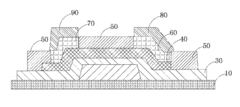
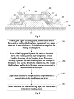
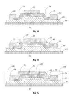
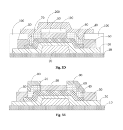
Metal oxide thin-film transistor, method of fabricating the same, and array substrate
PatentInactiveUS9634036B1
Innovation
- A metal oxide TFT with a blocking spread layer doped with boron ions and/or phosphorus ions, composed of molybdenum and titanium, is used to prevent copper diffusion, with a thickness ranging from 100 to 500 Å and a doping concentration of 10% to 90%, which improves the blocking efficiency.
Oxide semiconductor thin-film and thin-film transistor consisted thereof
PatentActiveUS11677031B2
Innovation
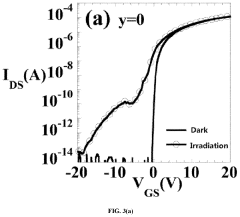
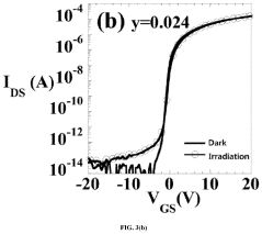
- Doping rare-earth oxides such as praseodymium, terbium, dysprosium, or ytterbium into metal oxide semiconductors to act as light stabilizers, shifting the band structure from direct to indirect gap, reducing photo-induced carriers and maintaining threshold voltage stability under light irradiation without degrading mobility.
IP Strategy and Licensing Considerations
The intellectual property landscape surrounding metal oxide TFT technology represents a complex ecosystem that requires strategic navigation. Key patent holders including Samsung, LG Display, Sharp, and various academic institutions have established robust IP portfolios covering fundamental aspects of metal oxide semiconductor composition, device structures, and manufacturing processes. Organizations seeking to develop or implement this technology must adopt comprehensive IP strategies that balance risk management with innovation opportunities.
Cross-licensing agreements have emerged as a predominant strategy within the display industry, particularly for metal oxide TFT technology. These arrangements allow companies to access essential patents while reducing litigation risks and associated costs. Notable examples include strategic partnerships between major display manufacturers and semiconductor companies that have facilitated broader technology adoption while ensuring appropriate compensation for innovation investments.
Patent pooling represents another viable approach for managing the dense patent landscape. By aggregating related patents from multiple owners into a single licensing platform, these pools can significantly reduce transaction costs and mitigate fragmentation issues. For emerging players in the metal oxide TFT space, careful evaluation of existing patent pools and their licensing terms is essential before committing to specific technology implementations.
Freedom-to-operate (FTO) analysis must be conducted systematically before significant R&D investments or product launches. This process involves identifying potentially blocking patents, assessing their validity and scope, and developing appropriate mitigation strategies. Companies should establish regular FTO review processes that align with product development timelines to avoid costly redesigns or legal challenges.
Defensive patenting strategies remain crucial even for organizations primarily implementing rather than developing core technologies. Building strategic patent portfolios around implementation-specific innovations, manufacturing improvements, or application-specific adaptations can provide valuable bargaining chips in licensing negotiations and protect market differentiation.
Geographic considerations significantly impact licensing strategies, with different enforcement regimes across major markets including the US, EU, China, Japan, and South Korea. Companies must develop region-specific approaches that account for variations in patent examination standards, enforcement mechanisms, and remedies available to patent holders.
Competitive Patent Positioning
The competitive patent landscape for metal oxide TFT technology reveals a complex ecosystem dominated by several key players who have established strong intellectual property portfolios. Samsung Display and LG Display maintain dominant positions with extensive patent coverage across fundamental metal oxide semiconductor compositions, device structures, and manufacturing processes. Their strategic patent filings focus on IGZO (Indium Gallium Zinc Oxide) formulations and novel device architectures that enhance electron mobility while maintaining stability.
Sharp Corporation and Japan Display Inc. have developed significant patent portfolios specifically targeting oxide TFT backplane technologies for high-resolution displays. Their intellectual property emphasizes specialized passivation techniques and interface engineering methods that mitigate threshold voltage instability issues common in metal oxide TFTs.
In the semiconductor manufacturing equipment sector, Applied Materials and Tokyo Electron hold critical patents covering deposition techniques for uniform metal oxide films, particularly those involving sputtering and atomic layer deposition methodologies. These patents represent potential bottlenecks for new market entrants seeking to establish manufacturing capabilities.
Chinese companies including BOE Technology and CSOT have rapidly expanded their patent portfolios over the past five years, focusing primarily on application-specific implementations and manufacturing cost reduction. Their intellectual property strategy appears to emphasize incremental innovations that circumvent established patents while developing region-specific manufacturing advantages.
Academic institutions including Taiwan's ITRI and Korea's KAIST maintain influential patent positions in next-generation metal oxide materials, including amorphous mixed metal oxides and solution-processed variants. These patents often represent early-stage technologies with potential to disrupt current manufacturing paradigms.
Analysis of citation networks reveals that patents related to hydrogen diffusion control and oxygen vacancy management in metal oxide films receive disproportionately high citation rates, indicating their fundamental importance to the technology. Companies controlling these foundational patents often leverage them for cross-licensing agreements that shape industry partnerships.
The geographical distribution of patent filings shows concentration in East Asia, with increasing activity in the United States focused on specialized applications including transparent electronics and flexible displays. European patent activity remains focused on materials science innovations rather than device architecture or manufacturing processes.
Unlock deeper insights with Patsnap Eureka Quick Research — get a full tech report to explore trends and direct your research. Try now!
Generate Your Research Report Instantly with AI Agent
Supercharge your innovation with Patsnap Eureka AI Agent Platform!