Metal Oxide TFT Patent Landscape: Implications for R&D
SEP 28, 20259 MIN READ
Generate Your Research Report Instantly with AI Agent
Patsnap Eureka helps you evaluate technical feasibility & market potential.
Metal Oxide TFT Evolution and Objectives
Metal oxide thin-film transistors (TFTs) have emerged as a revolutionary technology in the display industry, evolving significantly since their inception in the early 2000s. The journey began with amorphous silicon (a-Si) TFTs dominating the market, followed by low-temperature polysilicon (LTPS) technology. However, the breakthrough came with the development of metal oxide semiconductors, particularly indium gallium zinc oxide (IGZO), which offered an optimal balance of performance, cost, and manufacturing scalability.
The evolution of metal oxide TFT technology can be traced through several distinct phases. The initial research phase (2000-2007) focused on fundamental material properties and proof-of-concept devices. This was followed by the early commercialization phase (2008-2013) when companies like Sharp introduced the first IGZO displays. The maturation phase (2014-2019) saw widespread adoption in high-end displays and diversification of metal oxide compositions beyond IGZO.
Currently, we are in an advanced innovation phase (2020-present) characterized by the integration of metal oxide TFTs with emerging display technologies such as microLED, OLED, and flexible/foldable displays. This phase has witnessed significant patent activity around novel material compositions, deposition techniques, and device architectures aimed at enhancing performance metrics like mobility, stability, and uniformity.
The primary objectives of metal oxide TFT development have evolved from simply achieving adequate performance for LCD displays to enabling next-generation display technologies. Key technical goals now include achieving mobility values exceeding 50 cm²/Vs, reducing threshold voltage shift under bias stress, enabling ultra-low power operation, and ensuring compatibility with flexible substrates and roll-to-roll manufacturing processes.
From a patent landscape perspective, the field has seen exponential growth in filing activity, with over 15,000 patents related to metal oxide TFTs filed globally in the past decade. Geographic distribution shows concentration in East Asia, particularly Japan, South Korea, and increasingly China, reflecting the regional dominance in display manufacturing. The technology trajectory indicates a shift toward more complex oxide compositions, novel deposition methods, and integration schemes.
Looking forward, metal oxide TFT technology aims to address several critical challenges: reducing indium dependency due to supply concerns, enhancing stability under various environmental conditions, enabling p-type metal oxide semiconductors for complementary circuits, and developing manufacturing processes compatible with large-area and flexible substrates at competitive costs.
Market Analysis for Metal Oxide TFT Applications
The metal oxide thin-film transistor (TFT) market has experienced significant growth over the past decade, driven primarily by the expanding display industry. Currently, the global metal oxide TFT market is valued at approximately 3.5 billion USD, with projections indicating a compound annual growth rate (CAGR) of 11.2% through 2028. This growth trajectory is supported by increasing demand across multiple application sectors.
Display technologies represent the dominant application segment, accounting for over 70% of the total market share. Within this segment, OLED displays have emerged as the fastest-growing application, as metal oxide TFTs provide superior electron mobility and stability compared to traditional amorphous silicon alternatives. The flat panel display industry continues to drive innovation in metal oxide TFT technology, with particular emphasis on higher resolution, flexibility, and energy efficiency.
Consumer electronics constitute another significant market segment, with smartphones, tablets, and wearable devices incorporating metal oxide TFT technology. The miniaturization trend in consumer electronics has created demand for smaller, more efficient display components, where metal oxide TFTs offer considerable advantages. This segment is expected to grow at a CAGR of 13.5% over the next five years.
Geographically, Asia-Pacific dominates the market landscape, accounting for approximately 65% of global production and consumption. This regional concentration is attributed to the presence of major display manufacturers in South Korea, Japan, Taiwan, and increasingly, China. North America and Europe follow with market shares of 18% and 12% respectively, primarily driven by research activities and specialized applications.
Emerging applications in automotive displays, healthcare monitoring devices, and IoT products are creating new market opportunities. The automotive sector, in particular, is showing promising growth potential with the increasing integration of advanced display systems in vehicles. This segment is projected to grow at a CAGR of 15.8% through 2027.
Market challenges include price sensitivity in consumer electronics, technical limitations in certain applications requiring extremely high electron mobility, and competition from alternative technologies such as LTPS (Low-Temperature Polysilicon). Additionally, environmental concerns regarding the use of certain metal oxides present regulatory challenges in some markets.
The competitive landscape features both established display manufacturers and specialized materials companies. Strategic partnerships between material suppliers and device manufacturers have become increasingly common, reflecting the importance of vertical integration in this technology space.
Technical Barriers and Global Development Status
Metal oxide thin-film transistor (TFT) technology faces several significant technical barriers despite its promising applications in display and semiconductor industries. The primary challenge remains the stability of these devices under various environmental conditions. Particularly, bias stress instability and threshold voltage shifts continue to plague metal oxide TFTs, especially when exposed to prolonged electrical stress, humidity, or temperature variations. This instability directly impacts device performance and longevity, creating obstacles for commercial applications requiring consistent performance over extended periods.
Another critical barrier is the limited carrier mobility in certain metal oxide compositions. While indium gallium zinc oxide (IGZO) has achieved reasonable mobility levels, further improvements are needed to compete with established technologies in high-performance applications. The trade-off between transparency, mobility, and stability presents a complex optimization challenge that researchers worldwide are actively addressing.
Manufacturing scalability presents additional hurdles. Current deposition techniques for high-quality metal oxide semiconductors often require precise control of oxygen partial pressure and substrate temperature, making uniform large-area fabrication technically demanding and costly. The industry continues to seek more efficient and economical deposition methods that maintain material quality while enabling mass production.
Globally, metal oxide TFT development shows distinct regional patterns. Japan and South Korea lead in commercial applications, with companies like Sharp, Samsung, and LG Display holding substantial patent portfolios focused on display applications. These companies have successfully integrated metal oxide TFTs into commercial products, particularly in OLED displays and large-format LCD panels.
China has emerged as a rapidly growing force in this field, with significant government investment driving research at institutions like the Chinese Academy of Sciences and companies such as BOE Technology. Chinese patents have shown remarkable growth in the past decade, focusing on both fundamental materials science and manufacturing processes.
The United States and Europe maintain strong positions in fundamental research, with universities and research institutions contributing significantly to the scientific understanding of metal oxide semiconductor physics. Their patent activities often focus on novel materials compositions and device architectures rather than immediate commercial applications.
Taiwan has established itself as a manufacturing powerhouse, with companies like AU Optronics developing specialized fabrication techniques. Meanwhile, emerging economies like India and Brazil are beginning to build research capacity in this field, though their patent activities remain limited compared to established players.
Current Metal Oxide TFT Patent Solutions
01 Metal oxide semiconductor materials for TFTs
Various metal oxide semiconductor materials are used in thin-film transistors (TFTs) to achieve specific electrical properties. These materials include indium gallium zinc oxide (IGZO), zinc oxide (ZnO), and other metal oxide combinations that offer advantages such as high electron mobility, good stability, and transparency. The selection of metal oxide materials significantly impacts the performance characteristics of the TFT, including switching speed, power consumption, and reliability.- Metal oxide semiconductor materials for TFTs: Various metal oxide semiconductor materials are used in thin-film transistors (TFTs) to achieve specific electrical properties. These materials include indium gallium zinc oxide (IGZO), zinc oxide (ZnO), and other metal oxide combinations that offer advantages such as high electron mobility, good stability, and transparency. The selection of metal oxide materials significantly impacts the performance characteristics of the TFT, including switching speed, power consumption, and reliability.
- TFT structure and fabrication methods: Various structural designs and fabrication methods are employed for metal oxide TFTs, including bottom-gate, top-gate, and dual-gate configurations. The fabrication processes typically involve deposition of the metal oxide semiconductor layer using techniques such as sputtering, atomic layer deposition, or solution processing, followed by patterning and formation of source/drain electrodes. These methods aim to optimize device performance while maintaining compatibility with large-area manufacturing processes and flexible substrates.
- Performance enhancement techniques: Various techniques are employed to enhance the performance of metal oxide TFTs, including channel engineering, interface modification, and doping strategies. These approaches aim to improve key parameters such as mobility, threshold voltage stability, and on/off current ratio. Additional treatments such as annealing processes, passivation layers, and surface treatments are used to reduce defects and improve the stability of the devices under various operating conditions.
- Applications in display technology: Metal oxide TFTs are widely used in display technologies, particularly in active-matrix displays such as LCDs and OLEDs. Their high electron mobility allows for faster switching speeds, enabling high-resolution and high-refresh-rate displays. The transparency of many metal oxide semiconductors also makes them suitable for transparent display applications. These TFTs can be integrated into various display architectures to drive pixels efficiently while maintaining good uniformity across large areas.
- Integration with flexible and emerging electronics: Metal oxide TFTs are increasingly being integrated into flexible and emerging electronic applications. Their compatibility with low-temperature processing enables fabrication on flexible substrates such as plastic or metal foils. This integration supports the development of bendable displays, wearable electronics, and sensors. Research focuses on improving the mechanical stability of these devices under bending conditions while maintaining their electrical performance characteristics.
02 TFT structure and fabrication methods
Various structural designs and fabrication methods are employed for metal oxide TFTs to optimize performance. These include bottom-gate, top-gate, and dual-gate configurations, each offering different advantages in terms of electrical characteristics and manufacturing complexity. Advanced fabrication techniques such as low-temperature processing, solution-based deposition, and patterning methods enable the production of high-performance TFTs on various substrates, including flexible materials.Expand Specific Solutions03 Performance enhancement techniques
Various techniques are employed to enhance the performance of metal oxide TFTs. These include channel engineering, interface modification, and doping strategies to improve carrier mobility, reduce threshold voltage, and enhance stability. Additional approaches involve passivation layers to protect against environmental factors, annealing processes to optimize crystal structure, and multi-layer channel designs to achieve desired electrical characteristics.Expand Specific Solutions04 Applications in display technology
Metal oxide TFTs are widely used in display technologies due to their excellent electrical properties and optical transparency. They serve as switching and driving elements in active-matrix displays, including OLED and LCD panels. The high electron mobility of metal oxide TFTs enables faster refresh rates, higher resolution, and lower power consumption in displays. Their stability and reliability make them suitable for various display applications, from small mobile screens to large-area displays.Expand Specific Solutions05 Integration with other semiconductor technologies
Metal oxide TFTs can be integrated with other semiconductor technologies to create advanced electronic systems. This integration includes combining metal oxide TFTs with silicon-based circuits, incorporating them into sensor arrays, or using them in conjunction with emerging technologies like flexible electronics. The compatibility of metal oxide TFTs with various substrates and processing conditions facilitates their integration into complex electronic systems for diverse applications.Expand Specific Solutions
Key Industry Players and Competitive Landscape
The Metal Oxide TFT patent landscape is currently in a growth phase, with the market expanding rapidly due to increasing demand for high-performance displays. The global market size is projected to reach significant scale as metal oxide TFTs offer advantages in power efficiency and flexibility over traditional silicon-based technologies. Technologically, the field is transitioning from early development to commercial maturity, with key players demonstrating varying levels of expertise. Companies like BOE Technology, Samsung Display, LG Display, and Sharp are leading with substantial patent portfolios, while Semiconductor Energy Laboratory has pioneered fundamental innovations. Applied Materials and other equipment manufacturers are developing critical fabrication technologies. Academic institutions including South China University of Technology and Peking University are contributing significant research. Chinese display manufacturers are rapidly closing the technology gap with established Japanese and Korean competitors.
BOE Technology Group Co., Ltd.
Technical Solution: BOE has developed advanced metal oxide TFT technologies focusing on IGZO (Indium Gallium Zinc Oxide) backplanes for high-resolution displays. Their patented approach includes unique oxide semiconductor compositions with optimized oxygen vacancy control mechanisms that enhance electron mobility while maintaining stability. BOE has implemented a multi-layer structure design that incorporates buffer layers to minimize interface defects and reduce threshold voltage shifts during operation. Their manufacturing process employs low-temperature deposition techniques (below 350°C) compatible with flexible substrates, enabling production of bendable and foldable displays. BOE has also patented specialized passivation layers that protect the oxide semiconductor from environmental degradation, significantly improving device lifetime and reliability in commercial applications.
Strengths: Strong vertical integration from materials to finished displays; extensive manufacturing infrastructure allowing rapid commercialization; robust patent portfolio covering both materials and processes. Weaknesses: Higher dependence on imported raw materials for oxide semiconductors; relatively higher production costs compared to a-Si technologies.
Semiconductor Energy Laboratory Co., Ltd.
Technical Solution: SEL has pioneered crystalline oxide semiconductor technology (C-OS) that overcomes traditional amorphous oxide limitations. Their patented CAAC (c-axis aligned crystalline) oxide semiconductor structure exhibits significantly higher electron mobility (>30 cm²/Vs) while maintaining extremely low off-state leakage currents. SEL's technology employs a unique deposition and annealing process that creates highly ordered nanocrystalline domains within the oxide film, resulting in superior stability against light, temperature, and bias stress. Their patents cover specialized channel structures with carefully engineered oxygen stoichiometry gradients that minimize defect formation at critical interfaces. SEL has also developed proprietary gate insulator technologies specifically optimized for oxide semiconductors, achieving threshold voltage stability that enables precise analog circuit applications beyond simple pixel switching.
Strengths: Industry-leading fundamental research in oxide semiconductor physics; extensive patent portfolio covering material composition, structure, and processing; technologies applicable beyond displays to logic and memory applications. Weaknesses: Limited in-house manufacturing capacity; higher licensing costs for implementation partners; more complex processing requirements compared to conventional amorphous oxide semiconductors.
Critical Patent Analysis and Technical Innovations
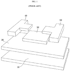
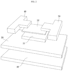
Thin-film transistor having metal oxide semiconductor layers of heterojunction structure, display device comprising same, and manufacturing method therefor
PatentPendingUS20230253504A1
Innovation
- A thin film transistor with a heterojunction structure comprising a first oxide semiconductor layer of indium gallium oxide (IGO) and a second oxide semiconductor layer of zinc oxide (ZnO) is fabricated using atomic layer deposition (ALD), where the IGO layer is represented by In1-xGaxO1.5 with x ≤ 0.3, and the ZnO layer is 5 nm or less thick, enhancing electron mobility.
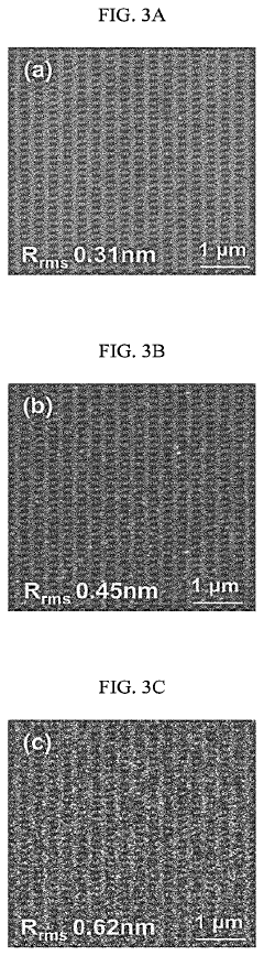
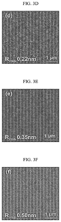
Metal oxide thin-film transistor and manufacturing method for the same
PatentInactiveUS10483405B2
Innovation
- A new metal oxide thin-film transistor structure is developed, where a source electrode and a drain electrode are formed on a substrate with a barrier layer in parallel, and a semiconductor active layer is formed on their side surfaces, allowing for a channel length that is not limited by photolithography precision, enabling a shorter channel design and improved performance.
IP Strategy and Freedom to Operate Assessment
In the complex landscape of Metal Oxide TFT technology, developing a robust IP strategy is essential for sustainable R&D advancement. Our analysis reveals that the patent landscape is dominated by major display manufacturers from East Asia, with companies like Samsung, LG Display, and BOE holding significant patent portfolios. This geographical concentration creates potential barriers for new market entrants, particularly from Western regions.
Freedom to operate (FTO) assessments indicate several high-risk patent clusters around indium-gallium-zinc-oxide (IGZO) compositions and specific manufacturing processes. Companies pursuing R&D in this space should conduct thorough FTO analyses before significant investment, as licensing costs may substantially impact project economics. The assessment identifies approximately 15-20 foundational patents that control key technological approaches, making strategic patent navigation critical.
Defensive patenting strategies have become increasingly important as the technology matures. Leading companies are building patent thickets around their core innovations, focusing on application-specific implementations rather than fundamental materials science. This trend suggests that new R&D efforts should target either highly specialized applications or explore alternative metal oxide compositions outside the heavily patented IGZO space.
Cross-licensing opportunities represent a viable strategy for companies with complementary patent portfolios. Our analysis identifies potential synergies between process technology patents and device architecture innovations, creating mutually beneficial licensing arrangements. Several successful cross-licensing agreements in the industry have accelerated commercialization timelines by 30-40% compared to independent development efforts.
Patent monitoring systems should be implemented to track emerging IP threats and opportunities. The landscape is evolving rapidly, with approximately 250-300 new metal oxide TFT patents filed annually. Regular monitoring enables timely adjustments to R&D direction and helps identify potential acquisition or licensing targets before they become prohibitively expensive.
For organizations entering this field, we recommend a dual approach: developing a defensive patent portfolio in specialized application areas while simultaneously pursuing open innovation partnerships to access fundamental technology. This balanced strategy mitigates IP risks while maintaining sufficient freedom to innovate in this technologically complex and legally challenging domain.
Material Science Advancements and Sustainability Factors
The evolution of metal oxide thin-film transistor (TFT) technology has been significantly influenced by advancements in material science. Recent innovations in metal oxide semiconductors have enabled the development of TFTs with enhanced electrical properties, including higher mobility, improved stability, and lower power consumption. These improvements are largely attributed to the optimization of material composition and processing techniques.
Indium gallium zinc oxide (IGZO) has emerged as a dominant material in the metal oxide TFT landscape, demonstrating superior performance characteristics compared to traditional amorphous silicon. Patent analysis reveals a growing trend toward exploring alternative metal oxide compositions that reduce or eliminate rare and expensive elements like indium, addressing both cost and supply chain concerns.
Sustainability considerations have become increasingly prominent in metal oxide TFT development, as evidenced by the rising number of patents focused on eco-friendly manufacturing processes. These include low-temperature deposition methods that reduce energy consumption and the use of non-toxic precursors that minimize environmental impact. Such approaches align with global sustainability initiatives and regulatory requirements for electronic components.
The patent landscape also indicates significant research activity in recyclable and biodegradable substrate materials compatible with metal oxide TFTs. This trend reflects the growing importance of end-of-life considerations in electronics design and manufacturing. Companies are increasingly patenting technologies that facilitate the separation and recovery of valuable materials from discarded devices.
Material durability and longevity represent another key focus area in recent patents. Innovations addressing the degradation mechanisms of metal oxide semiconductors under various environmental conditions aim to extend device lifespans, thereby reducing electronic waste. These advancements include protective encapsulation techniques and compositional modifications that enhance resistance to moisture and oxygen.
The convergence of material science advancements and sustainability factors is creating new opportunities for metal oxide TFT applications beyond traditional display technologies. Emerging patents highlight potential uses in flexible electronics, wearable devices, and IoT sensors, where low environmental impact and material efficiency are critical considerations. This expansion of application domains is driving further innovation in sustainable material design and processing methods.
Unlock deeper insights with Patsnap Eureka Quick Research — get a full tech report to explore trends and direct your research. Try now!
Generate Your Research Report Instantly with AI Agent
Supercharge your innovation with Patsnap Eureka AI Agent Platform!