Metal Oxide TFTs: Licensing Insights and Market Opportunities
SEP 28, 20259 MIN READ
Generate Your Research Report Instantly with AI Agent
Patsnap Eureka helps you evaluate technical feasibility & market potential.
Metal Oxide TFT Evolution and Objectives
Metal oxide thin-film transistors (TFTs) have evolved significantly since their inception in the early 2000s, transforming from laboratory curiosities to commercial display technologies. The journey began with the pioneering work on transparent amorphous oxide semiconductors by Hosono's group at Tokyo Institute of Technology in 2004, demonstrating that amorphous InGaZnO (a-IGZO) could achieve electron mobilities over ten times higher than amorphous silicon while maintaining excellent uniformity and stability.
The evolution of metal oxide TFTs can be divided into distinct technological generations. First-generation devices focused on a-IGZO for large-area displays, while second-generation developments expanded material compositions to include ZnO, InZnO, and HfInZnO systems, optimizing for specific performance metrics. The current third generation explores novel architectures, ultra-thin films, and advanced deposition techniques to enhance performance parameters including mobility, stability, and operational voltage.
Market adoption has followed a clear trajectory, with initial implementation in high-end displays followed by broader adoption in mid-range consumer electronics. The technology has progressively displaced amorphous silicon in applications requiring higher resolution, faster refresh rates, and lower power consumption. This transition has been particularly evident in the mobile device sector, where metal oxide TFTs enable higher pixel densities while reducing power requirements.
The primary technical objectives driving metal oxide TFT development include achieving higher electron mobility (targeting >30 cm²/Vs in commercial products), enhancing operational stability under bias stress conditions, reducing manufacturing costs through simplified processes, and enabling new form factors through flexibility and transparency. Additionally, there is growing interest in developing p-type oxide semiconductors to complement the predominantly n-type materials currently available, potentially enabling complementary oxide electronics.
Environmental considerations have also shaped the technology's evolution, with research increasingly focused on reducing or eliminating rare and toxic elements like indium while maintaining performance. This has led to exploration of alternative compositions based on more abundant elements such as zinc, tin, and aluminum.
Looking forward, the technology roadmap aims to position metal oxide TFTs as the dominant backplane technology for next-generation displays, including transparent, flexible, and stretchable formats. Concurrently, there is growing interest in expanding applications beyond displays into areas such as sensors, logic circuits, and memory devices, which would significantly broaden the technology's market impact and licensing value.
Market Demand Analysis for Metal Oxide TFTs
The global market for Metal Oxide Thin-Film Transistors (TFTs) has experienced significant growth in recent years, primarily driven by the expanding display industry. The demand for Metal Oxide TFTs, particularly Indium Gallium Zinc Oxide (IGZO) and Zinc Oxide (ZnO) variants, has been steadily increasing due to their superior performance characteristics compared to traditional amorphous silicon (a-Si) TFTs.
The display panel market, valued at approximately $150 billion in 2022, represents the largest application segment for Metal Oxide TFTs. Industry forecasts project this market to grow at a compound annual growth rate (CAGR) of 7.8% through 2028, with Metal Oxide TFTs capturing an increasing share from conventional technologies. This growth is particularly evident in high-resolution displays, where Metal Oxide TFTs' higher electron mobility enables faster switching speeds and improved pixel densities.
Consumer electronics remains the dominant end-use sector, with smartphones, tablets, and televisions accounting for over 70% of Metal Oxide TFT demand. The trend toward larger, higher-resolution displays in these devices continues to fuel market expansion. Additionally, the automotive industry has emerged as a rapidly growing segment, with in-vehicle displays increasingly adopting Metal Oxide TFT technology for enhanced performance in varying light conditions.
Regionally, East Asia dominates both production and consumption of Metal Oxide TFTs, with China, Japan, South Korea, and Taiwan collectively representing over 80% of global market share. However, emerging markets in Southeast Asia and India are showing accelerated growth rates as display manufacturing facilities expand into these regions.
The transition to flexible and foldable displays represents a significant market opportunity for Metal Oxide TFTs. Their compatibility with low-temperature processing makes them ideal for flexible substrates, with market analysts predicting the flexible display segment to grow at a CAGR of 35% through 2027, reaching a market value of $30 billion.
Energy efficiency requirements are also driving demand, as Metal Oxide TFTs consume significantly less power than traditional technologies. This aligns with global sustainability initiatives and consumer preferences for longer battery life in portable devices. Market research indicates that energy efficiency is now among the top three purchasing considerations for consumers of premium electronic devices.
Licensing opportunities in the Metal Oxide TFT space are expanding as the technology matures. Patent analytics reveal over 5,000 active patents related to Metal Oxide TFT technology, with licensing revenues estimated to exceed $500 million annually. Companies with strong IP portfolios in this domain are increasingly monetizing their assets through strategic licensing agreements rather than solely through manufacturing.
Technical Landscape and Barriers
Metal oxide thin-film transistors (TFTs) have emerged as a transformative technology in the display industry, positioned between amorphous silicon (a-Si) and low-temperature polysilicon (LTPS) in terms of performance and cost. The global landscape for metal oxide TFT technology is characterized by significant regional variations in development focus and implementation strategies.
In Asia, particularly Japan, South Korea, and Taiwan, substantial advancements have been made in metal oxide TFT technology, with companies like Sharp, Samsung, and LG Display leading commercial applications. These regions benefit from established semiconductor manufacturing ecosystems and government support for display technologies. China has rapidly expanded its capabilities, with BOE Technology and TCL CSOT making significant investments in metal oxide TFT production lines.
North America and Europe maintain strong positions in fundamental research and intellectual property development, though commercial manufacturing has largely shifted to Asia. Universities and research institutions in these regions continue to pioneer novel materials and device architectures that could shape future generations of metal oxide TFTs.
Despite impressive progress, several technical barriers persist in metal oxide TFT development. Stability issues remain a primary concern, particularly under prolonged bias stress and varying environmental conditions. Threshold voltage shifts and mobility degradation over time can significantly impact device performance and longevity. Additionally, achieving consistent electrical characteristics across large-area substrates presents manufacturing challenges that limit yield rates.
The integration of metal oxide TFTs with emerging display technologies such as microLED and OLED displays introduces additional complexities. Current limitations in achieving p-type metal oxide semiconductors with performance comparable to n-type materials restrict the development of complementary circuits, necessitating more complex circuit designs.
Scaling challenges also exist as pixel densities increase for high-resolution displays. The industry faces difficulties in maintaining performance while reducing device dimensions, particularly for applications requiring ultra-high definition or high refresh rates. Furthermore, the environmental impact of certain metal oxide materials, including indium scarcity and potential toxicity concerns with some compounds, presents sustainability challenges.
Manufacturing processes for metal oxide TFTs still require optimization to reduce costs and increase throughput. The balance between performance enhancement and manufacturing simplicity remains a key consideration for widespread adoption. Solution-processing methods show promise for cost reduction but currently lag behind vacuum-based techniques in device performance and reliability.
Intellectual property landscapes present additional barriers, with complex patent thickets surrounding key materials and processes. This complexity creates licensing challenges for new market entrants and can impede innovation in certain application areas.
Current Metal Oxide TFT Solutions
01 Metal oxide semiconductor materials for TFTs
Various metal oxide semiconductor materials can be used in thin-film transistors (TFTs) to achieve specific electrical properties. These materials include zinc oxide (ZnO), indium gallium zinc oxide (IGZO), and other metal oxide combinations that offer advantages such as high electron mobility, good stability, and transparency. The selection of appropriate metal oxide materials is crucial for optimizing TFT performance in display and electronic applications.- Metal oxide semiconductor materials for TFTs: Various metal oxide semiconductor materials are used in thin-film transistors (TFTs) to achieve specific electrical properties. These materials include zinc oxide (ZnO), indium gallium zinc oxide (IGZO), and other metal oxide combinations that offer advantages such as high electron mobility, good stability, and transparency. The selection of metal oxide materials significantly impacts the performance characteristics of the TFTs, including switching speed, power consumption, and reliability.
- Fabrication methods for metal oxide TFTs: Various fabrication techniques are employed to manufacture metal oxide TFTs, including sputtering, atomic layer deposition (ALD), solution processing, and chemical vapor deposition (CVD). These methods control the crystallinity, composition, and interface quality of the metal oxide layers, which directly affect device performance. Post-deposition treatments such as annealing in different atmospheres are also used to optimize the electrical properties and stability of the metal oxide semiconductor layer.
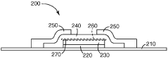
- Device structures and architectures for metal oxide TFTs: Different device structures are implemented for metal oxide TFTs, including bottom-gate, top-gate, dual-gate, and self-aligned configurations. Each architecture offers specific advantages in terms of performance, manufacturing complexity, and integration capability. The design of source/drain electrodes, gate dielectrics, and channel regions significantly impacts the electrical characteristics of the TFTs, including threshold voltage, subthreshold swing, and on/off current ratio.
- Integration of metal oxide TFTs in display technologies: Metal oxide TFTs are widely integrated into various display technologies, including LCD, OLED, and microLED displays. Their high electron mobility and good uniformity make them suitable for driving pixels in high-resolution displays. The integration process involves specific design considerations to ensure compatibility with display manufacturing processes and to achieve desired performance metrics such as refresh rate, power consumption, and pixel density.
- Performance enhancement techniques for metal oxide TFTs: Various techniques are employed to enhance the performance of metal oxide TFTs, including interface engineering, doping strategies, and multilayer channel structures. These approaches aim to improve key parameters such as carrier mobility, stability under bias stress, and uniformity across large areas. Additional methods include passivation layers to protect against environmental degradation, optimized gate dielectrics to reduce interface traps, and novel contact materials to reduce contact resistance.
02 Fabrication methods for metal oxide TFTs
Various fabrication techniques are employed to manufacture metal oxide TFTs with improved performance characteristics. These methods include solution processing, sputtering, atomic layer deposition, and annealing treatments. The fabrication process significantly influences the crystallinity, interface quality, and overall performance of the metal oxide semiconductor layer. Optimized fabrication methods can reduce defects and enhance the stability and reliability of the resulting TFTs.Expand Specific Solutions03 Device structures and architectures for metal oxide TFTs
Different structural configurations and architectures are implemented in metal oxide TFTs to enhance performance and functionality. These include bottom-gate, top-gate, dual-gate, and vertical structures, each offering specific advantages for different applications. The arrangement of electrodes, semiconductor layers, and dielectric materials significantly impacts the electrical characteristics and operational stability of the TFTs. Novel device architectures can address challenges such as threshold voltage instability and improve overall device performance.Expand Specific Solutions04 Integration of metal oxide TFTs in display technologies
Metal oxide TFTs are integrated into various display technologies, including LCD, OLED, and flexible displays. Their high electron mobility and transparency make them particularly suitable for these applications. The integration process involves addressing challenges related to uniformity, stability, and compatibility with existing manufacturing processes. Metal oxide TFTs enable higher resolution, faster refresh rates, and lower power consumption in display applications compared to conventional silicon-based TFTs.Expand Specific Solutions05 Performance enhancement techniques for metal oxide TFTs
Various techniques are employed to enhance the performance of metal oxide TFTs, including doping, interface engineering, and passivation treatments. These methods aim to improve carrier mobility, reduce threshold voltage, enhance stability, and minimize hysteresis effects. Additional approaches include the use of multilayer structures, composite materials, and novel dielectric materials. These enhancement techniques are crucial for meeting the demanding requirements of advanced electronic applications.Expand Specific Solutions
Key Industry Players and Ecosystem
Metal Oxide TFTs market is currently in a growth phase, with increasing adoption in display technologies. The market size is expanding rapidly, driven by demand for high-performance, low-power displays in consumer electronics and automotive applications. Technologically, the field is maturing with key players like BOE Technology Group, Semiconductor Energy Laboratory, and Applied Materials leading innovation. Chinese manufacturers including TCL China Star, Tianma Microelectronics, and InfoVision Optoelectronics are gaining significant market share, while research institutions like IMEC and South China University of Technology are advancing fundamental technologies. The competitive landscape shows a mix of established semiconductor companies and display manufacturers, with increasing focus on licensing opportunities as the technology becomes more mainstream for next-generation displays.
BOE Technology Group Co., Ltd.
Technical Solution: BOE has developed a proprietary metal oxide TFT technology platform called "GOA-free IGZO" (Gate-On-Array free Indium Gallium Zinc Oxide) that eliminates traditional gate driver ICs by integrating driving circuits directly into the display panel using their advanced oxide semiconductor process. Their technology achieves electron mobility of 15-20 cm²/Vs while maintaining ultra-low leakage current below 10^-13 A, enabling both high refresh rates (up to 144Hz) and low power consumption. BOE's manufacturing process incorporates specialized passivation layers and multi-step annealing techniques that significantly reduce oxygen vacancy fluctuations, resulting in threshold voltage stability improvement of approximately 40% compared to standard IGZO processes. Their metal oxide TFT backplanes support both LCD and OLED display technologies, with particular optimization for large-format 8K displays where the higher mobility enables narrower bezels and reduced power consumption. BOE has implemented this technology in production facilities across multiple generations (Gen 8.5, Gen 10.5) with high yields exceeding 90%.
Strengths: Vertical integration from material development to mass production; extensive manufacturing capacity across multiple fabs; proven high-volume production capability with competitive yields. Weaknesses: Relatively higher defect density compared to polysilicon alternatives; technology optimization primarily focused on display applications rather than broader semiconductor applications; some dependence on licensed IP from other players.
Semiconductor Energy Laboratory Co., Ltd.
Technical Solution: Semiconductor Energy Laboratory (SEL) has pioneered CAAC-IGZO (c-axis aligned crystalline indium-gallium-zinc oxide) technology for metal oxide TFTs. Their proprietary crystalline structure offers superior stability compared to conventional amorphous IGZO, with electron mobility exceeding 10 cm²/Vs while maintaining low off-state current below 10^-13 A. SEL has developed self-aligned top-gate structures that reduce parasitic capacitance by approximately 30%, enabling faster switching speeds for high-resolution displays. Their oxide semiconductor technology incorporates hydrogen barriers and specialized annealing processes that significantly reduce threshold voltage shift under bias stress conditions, extending device lifetime by over 50% compared to first-generation metal oxide TFTs. SEL's licensing model focuses on fundamental IP for oxide semiconductor composition and fabrication processes, with over 200 patents specifically covering IGZO implementation.
Strengths: Industry-leading stability and reliability metrics; comprehensive patent portfolio covering fundamental material science; established licensing relationships with major display manufacturers. Weaknesses: Higher manufacturing complexity compared to amorphous IGZO; requires specialized deposition equipment; relatively higher licensing costs compared to alternative TFT technologies.
Patent Analysis and IP Landscape
Stability enhancements in metal oxide semiconductor thin film transistors
PatentWO2010074927A2
Innovation
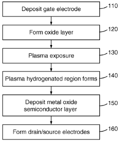
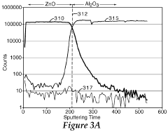
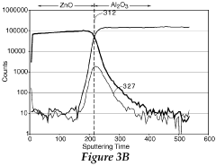
- Exposing the dielectric layer to a hydrogen-containing plasma before depositing the metal oxide semiconductor layer creates a hydrogenated region at the semiconductor-dielectric interface, enhancing carrier mobility and reducing hysteresis, thereby stabilizing the TFTs.
Thin film transistor with selectively doped oxide thin film
PatentActiveUS20190305133A1
Innovation
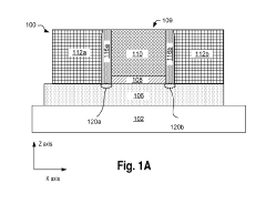
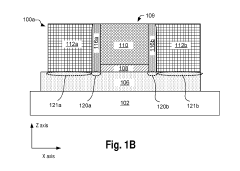
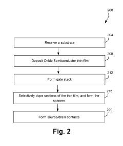
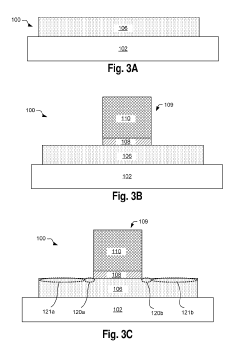
- Selectively doping sections of the channel underneath spacers and source/drain contacts with Arsenic, Phosphorus, and Antimony to reduce contact resistance and improve TFT performance.
Licensing Strategy and Models
In the rapidly evolving landscape of Metal Oxide TFT technology, establishing effective licensing strategies and models is crucial for both technology providers and adopters. The licensing ecosystem for Metal Oxide TFTs has matured significantly over the past decade, with several distinct models emerging as industry standards.
Patent pool licensing represents one of the most efficient approaches for Metal Oxide TFT technologies, allowing multiple patent holders to collectively license their intellectual property through a single entity. This model reduces transaction costs and mitigates litigation risks while providing licensees with comprehensive access to essential patents. Notable examples include the IGZO consortium, which has successfully implemented this approach for indium gallium zinc oxide technologies.
Exclusive licensing arrangements remain prevalent among research institutions and their commercial partners, particularly for novel oxide semiconductor compositions and fabrication techniques. These agreements typically include performance milestones, royalty structures based on production volumes, and field-of-use restrictions to maximize value for both parties while ensuring continued innovation.
Cross-licensing has become increasingly important as the Metal Oxide TFT ecosystem expands, with major display manufacturers exchanging access to complementary technologies. This approach has proven especially valuable for companies seeking to integrate Metal Oxide TFTs with other advanced display technologies such as OLED, micro-LED, or flexible substrates, creating comprehensive solution portfolios.
Tiered royalty structures have emerged as a preferred model for accommodating diverse market applications. These structures typically offer lower rates for high-volume, low-margin applications like standard displays, while implementing premium rates for specialized applications in medical imaging, automotive displays, or advanced sensing arrays where performance commands higher margins.
Open innovation platforms are gaining traction, particularly for process technologies and design tools. Several foundries now offer Metal Oxide TFT process design kits (PDKs) under reasonable licensing terms, fostering a broader ecosystem of designers and application developers while maintaining control over manufacturing processes.
Technology transfer packages have become sophisticated offerings that bundle patents, know-how, training, and ongoing support. These comprehensive packages are particularly valuable for emerging market manufacturers seeking to establish Metal Oxide TFT production capabilities, with licensing terms often including upfront fees, running royalties, and technical milestone payments.
As the market continues to diversify, hybrid licensing models that combine elements of these approaches are increasingly common, tailored to specific business relationships and technology applications. The most successful licensing strategies align incentives across the value chain while providing flexibility to adapt to rapidly evolving market conditions and technological developments.
Sustainability and Environmental Impact
Metal oxide TFTs represent a significant advancement in display technology with important sustainability implications across their entire lifecycle. The manufacturing processes for these transistors typically require lower temperatures compared to traditional silicon-based alternatives, resulting in substantial energy savings during production. This energy efficiency translates to reduced carbon emissions, making metal oxide TFT production more environmentally friendly than conventional semiconductor manufacturing.
The materials used in metal oxide TFTs also present environmental advantages. Many formulations utilize abundant elements such as zinc, indium, gallium, and tin, though concerns exist regarding the limited global supply of indium. Research into alternative compositions using more earth-abundant materials is actively progressing to address potential resource constraints and reduce reliance on rare elements.
During operation, displays incorporating metal oxide TFTs demonstrate superior energy efficiency, particularly in applications like e-readers and low-power displays. This efficiency extends device battery life and reduces overall energy consumption, contributing to decreased environmental impact throughout the product lifecycle. The potential for creating ultra-thin, flexible displays also enables material reduction in end products.
End-of-life considerations for metal oxide TFT technologies present both challenges and opportunities. While the diverse material composition can complicate recycling processes, their thin-film nature means they use significantly less material by volume compared to traditional semiconductor technologies. Industry stakeholders are developing specialized recycling techniques to recover valuable elements from discarded displays.
Several manufacturers have implemented green manufacturing initiatives specifically for metal oxide TFT production lines. These include closed-loop water systems, chemical usage reduction programs, and energy-efficient facility designs. Companies like Sharp, LG Display, and Samsung Display have published sustainability reports highlighting their progress in reducing the environmental footprint of their display manufacturing operations.
Regulatory frameworks worldwide are increasingly emphasizing electronic component sustainability. The European Union's Restriction of Hazardous Substances (RoHS) and Waste Electrical and Electronic Equipment (WEEE) directives directly impact metal oxide TFT manufacturing and disposal practices. Companies seeking to license or commercialize these technologies must navigate these evolving regulations, which can significantly influence market opportunities and technology adoption rates.
Unlock deeper insights with Patsnap Eureka Quick Research — get a full tech report to explore trends and direct your research. Try now!
Generate Your Research Report Instantly with AI Agent
Supercharge your innovation with Patsnap Eureka AI Agent Platform!