Metal Oxide TFTs' Role in Advanced Semiconductor Design
SEP 28, 20259 MIN READ
Generate Your Research Report Instantly with AI Agent
Patsnap Eureka helps you evaluate technical feasibility & market potential.
Metal Oxide TFTs Evolution and Objectives
Metal oxide thin-film transistors (TFTs) have evolved significantly since their inception in the early 2000s, transforming from experimental devices to critical components in modern display and semiconductor technologies. The journey began with amorphous silicon (a-Si) TFTs dominating the market, followed by the emergence of metal oxide semiconductors, particularly indium gallium zinc oxide (IGZO), which offered superior electron mobility and stability compared to their silicon counterparts.
The evolution of metal oxide TFTs can be traced through several key technological milestones. In 2003, researchers at Tokyo Institute of Technology demonstrated the first high-performance IGZO TFTs, achieving electron mobility exceeding 10 cm²/Vs at room temperature. This breakthrough represented a tenfold improvement over conventional a-Si TFTs. By 2012, commercial production of metal oxide TFT-based displays began, with Sharp Corporation pioneering IGZO displays for consumer electronics.
Recent advancements have focused on enhancing stability, reducing processing temperatures, and expanding application domains. The development of solution-processed metal oxide TFTs has enabled cost-effective manufacturing techniques compatible with flexible substrates. Concurrently, research into new metal oxide compositions, including zinc tin oxide (ZTO) and indium zinc oxide (IZO), has yielded devices with mobility values exceeding 50 cm²/Vs while maintaining excellent transparency.
The primary technical objectives for metal oxide TFTs in advanced semiconductor design center around several key areas. First, improving carrier mobility while maintaining low off-state current is crucial for high-performance, energy-efficient devices. Current research aims to achieve mobility values exceeding 100 cm²/Vs without compromising stability or introducing excessive leakage current.
Second, enhancing operational stability under various environmental conditions remains a significant challenge. This includes mitigating bias stress instability and improving resistance to humidity and temperature fluctuations, which are essential for reliable long-term operation in diverse applications.
Third, developing low-temperature processing techniques compatible with flexible substrates is vital for enabling next-generation flexible and wearable electronics. The goal is to achieve high-performance devices at processing temperatures below 200°C, allowing integration with temperature-sensitive materials and substrates.
Finally, scaling down device dimensions while maintaining performance metrics is essential for high-resolution displays and integrated circuit applications. This includes developing reliable patterning techniques at sub-micron scales and addressing the challenges of contact resistance that become increasingly significant at smaller dimensions.
Market Analysis for Metal Oxide TFT Applications
The metal oxide thin-film transistor (TFT) market is experiencing robust growth, driven by increasing demand for high-resolution displays and flexible electronics. The global metal oxide TFT market was valued at approximately $3.2 billion in 2022 and is projected to reach $7.5 billion by 2028, representing a compound annual growth rate (CAGR) of 15.3% during the forecast period.
Display applications currently dominate the metal oxide TFT market, accounting for over 70% of the total market share. Within this segment, OLED displays represent the fastest-growing application due to their superior performance characteristics and increasing adoption in premium smartphones and televisions. The transition from amorphous silicon (a-Si) to metal oxide semiconductors, particularly IGZO (Indium Gallium Zinc Oxide), has been accelerated by the industry's push toward higher resolution, lower power consumption, and improved refresh rates.
Beyond displays, emerging applications in flexible electronics, transparent electronics, and sensor arrays are creating new market opportunities. The flexible electronics segment is expected to grow at a CAGR of 22% through 2028, driven by innovations in wearable technology, foldable devices, and smart packaging. Metal oxide TFTs' compatibility with low-temperature processing makes them particularly suitable for these applications, where traditional silicon-based semiconductors face limitations.
Geographically, East Asia dominates the metal oxide TFT market, with Japan, South Korea, Taiwan, and China collectively accounting for approximately 65% of global production. This regional concentration is attributed to the strong presence of display manufacturers and semiconductor fabrication facilities. However, significant investments in North America and Europe are focused on specialized applications in medical imaging, automotive displays, and industrial sensors.
Consumer electronics remains the largest end-use industry for metal oxide TFTs, representing approximately 58% of market demand. However, automotive applications are showing the highest growth rate at 18.7% annually, driven by increasing integration of advanced display systems in vehicles and the transition toward electric and autonomous vehicles requiring sophisticated semiconductor solutions.
Key market challenges include supply chain vulnerabilities, particularly regarding indium availability and price volatility. Indium, a critical component in IGZO formulations, faces potential supply constraints due to its limited global reserves and geopolitical factors affecting mining and refining operations. This has prompted research into alternative metal oxide formulations with reduced dependence on rare elements.
Customer demand is increasingly focused on sustainability and energy efficiency, with metal oxide TFTs offering significant advantages in power consumption compared to conventional technologies. This aligns with global regulatory trends toward energy-efficient electronics and carbon footprint reduction in manufacturing processes.
Technical Barriers and Global Development Status
Metal oxide TFTs face several significant technical barriers that currently limit their widespread adoption in advanced semiconductor design. The most pressing challenge is the relatively low carrier mobility compared to conventional silicon-based transistors. While silicon transistors can achieve mobilities exceeding 100 cm²/Vs, metal oxide TFTs typically demonstrate mobilities in the range of 10-20 cm²/Vs, restricting their application in high-performance computing scenarios.
Stability issues present another major obstacle, particularly under prolonged bias stress and varying environmental conditions. Metal oxide semiconductors often exhibit threshold voltage shifts during extended operation, leading to inconsistent performance over time. This instability is exacerbated by sensitivity to ambient conditions, especially humidity and oxygen, which can significantly alter device characteristics.
The fabrication of complementary circuits remains problematic due to the inherent n-type nature of most metal oxide semiconductors. While n-type metal oxide TFTs have shown promising development, reliable p-type metal oxide semiconductors with comparable performance metrics have proven elusive, limiting the implementation of energy-efficient complementary circuit designs.
Globally, metal oxide TFT development shows distinct regional patterns. Japan has established itself as a pioneer in this field, with companies like Sharp and Sony leading commercial applications in display technologies. South Korean firms, particularly Samsung and LG Display, have made substantial investments in metal oxide TFT research, focusing on integration with OLED displays and flexible electronics.
In the United States, research efforts are primarily concentrated in academic institutions and national laboratories, with companies like Applied Materials developing manufacturing equipment rather than end products. The European landscape features strong academic research networks, particularly in Germany and the UK, often collaborating with Asian manufacturing partners to commercialize innovations.
China has rapidly emerged as a significant player, with substantial government investment supporting both academic research and industrial development. Companies like BOE Technology have made remarkable progress in incorporating metal oxide TFTs into commercial display products, challenging established Japanese and Korean manufacturers.
Recent global developments indicate a shift toward specialized applications rather than direct competition with silicon technology. Metal oxide TFTs are finding particular success in transparent electronics, flexible displays, and large-area sensor arrays where their unique properties offer advantages over conventional semiconductors. The technology has reached commercial maturity in display applications but remains in earlier development stages for more complex integrated circuits and specialized sensing applications.
Current Metal Oxide TFT Design Solutions
01 Metal oxide semiconductor materials for TFTs
Various metal oxide semiconductor materials can be used in thin-film transistors (TFTs) to achieve specific electrical properties. These materials include zinc oxide (ZnO), indium gallium zinc oxide (IGZO), and other metal oxide combinations that offer advantages such as high electron mobility, good stability, and transparency. The selection of appropriate metal oxide materials is crucial for determining the performance characteristics of the TFT devices.- Metal oxide semiconductor materials for TFTs: Various metal oxide semiconductor materials are used in thin-film transistors (TFTs) to achieve specific electrical properties. These materials include zinc oxide (ZnO), indium gallium zinc oxide (IGZO), and other metal oxide combinations that offer advantages such as high electron mobility, good stability, and transparency. The selection of metal oxide materials significantly impacts the performance characteristics of the TFT, including switching speed, power consumption, and reliability.
- Fabrication methods for metal oxide TFTs: Various fabrication techniques are employed to manufacture metal oxide TFTs, including sputtering, atomic layer deposition (ALD), solution processing, and chemical vapor deposition (CVD). These methods control the crystallinity, composition, and interface quality of the metal oxide layers. Post-deposition treatments such as annealing processes are often used to optimize the electrical properties of the metal oxide semiconductor layer and improve device performance.
- Device structures and architectures for metal oxide TFTs: Different structural configurations are implemented in metal oxide TFTs, including bottom-gate, top-gate, staggered, and coplanar architectures. Each structure offers specific advantages in terms of performance, manufacturing complexity, and integration capabilities. The design of source/drain electrodes, gate dielectrics, and channel regions significantly impacts device characteristics such as on/off ratio, threshold voltage, and subthreshold swing.
- Performance enhancement techniques for metal oxide TFTs: Various methods are employed to enhance the performance of metal oxide TFTs, including interface engineering, doping strategies, and multilayer channel structures. These techniques aim to improve carrier mobility, reduce threshold voltage, enhance stability, and minimize hysteresis effects. Passivation layers and encapsulation methods are also used to protect the devices from environmental factors and extend their operational lifetime.
- Applications of metal oxide TFTs in display and electronic devices: Metal oxide TFTs are widely used in various applications, particularly in display technologies such as OLED and LCD panels, where they serve as pixel-driving elements. Their unique combination of transparency, flexibility, and electrical performance makes them suitable for next-generation electronics including transparent displays, flexible electronics, and large-area sensors. The integration of metal oxide TFTs with other components enables the development of advanced electronic systems with improved functionality.
02 Fabrication methods for metal oxide TFTs
Various fabrication techniques are employed to create metal oxide TFTs, including sputtering, atomic layer deposition, solution processing, and thermal annealing. These methods affect the crystallinity, defect density, and interface quality of the metal oxide layers, which in turn influence the electrical performance of the TFTs. Optimization of fabrication parameters is essential to achieve desired TFT characteristics such as high mobility, low threshold voltage, and good stability.Expand Specific Solutions03 Device structures and architectures for metal oxide TFTs
Different structural configurations can be implemented for metal oxide TFTs, including bottom-gate, top-gate, staggered, and coplanar architectures. Each structure offers specific advantages in terms of performance, manufacturing complexity, and integration capability. The selection of appropriate gate dielectrics, electrode materials, and channel layer thickness also plays a crucial role in optimizing TFT performance for specific applications.Expand Specific Solutions04 Performance enhancement techniques for metal oxide TFTs
Various approaches can be employed to enhance the performance of metal oxide TFTs, including doping, multilayer channel structures, interface engineering, and passivation layers. These techniques aim to improve carrier mobility, reduce threshold voltage, enhance stability, and minimize hysteresis effects. Optimization of these parameters is essential for meeting the requirements of specific applications such as displays, sensors, and integrated circuits.Expand Specific Solutions05 Applications of metal oxide TFTs
Metal oxide TFTs find applications in various electronic devices due to their unique combination of transparency, flexibility, and electrical performance. They are widely used in active-matrix displays (LCDs, OLEDs), transparent electronics, flexible devices, sensors, and integrated circuits. The specific requirements of each application drive the optimization of TFT parameters such as mobility, on/off ratio, threshold voltage, and stability.Expand Specific Solutions
Leading Companies and Competitive Landscape
Metal oxide TFTs are emerging as a critical technology in advanced semiconductor design, with the market currently in a growth phase characterized by increasing adoption across display technologies. The global market is expanding rapidly, driven by demand for high-performance, energy-efficient displays in consumer electronics. Leading players include Samsung Display, LG Display, and BOE Technology Group, who are advancing the technology's maturity through significant R&D investments. Sharp and Semiconductor Energy Laboratory have pioneered IGZO (indium gallium zinc oxide) technology, while Applied Materials provides essential manufacturing equipment. Taiwan Semiconductor Manufacturing Co. and AUO Corp. are integrating metal oxide TFTs into their semiconductor ecosystems. The technology is approaching commercial maturity for display applications, with ongoing research focused on expanding into flexible electronics and next-generation computing architectures.
Semiconductor Energy Laboratory Co., Ltd.
Technical Solution: Semiconductor Energy Laboratory (SEL) has pioneered oxide semiconductor technology, particularly focusing on IGZO (Indium Gallium Zinc Oxide) TFTs. Their approach involves creating highly stable c-axis aligned crystalline (CAAC) IGZO structures that significantly reduce oxygen vacancies and carrier trapping. SEL has developed proprietary deposition techniques that enable precise control of film crystallinity and composition, resulting in TFTs with mobility exceeding 10 cm²/Vs while maintaining extremely low off-state leakage currents (below 10^-13 A) [1]. Their technology incorporates unique back-channel passivation methods and specialized annealing processes to enhance stability under negative bias temperature stress. SEL has successfully implemented these oxide TFTs in various applications including high-resolution displays, flexible electronics, and non-volatile memory circuits, demonstrating operational stability exceeding 10,000 hours under continuous stress conditions [2].
Strengths: Industry-leading stability and reliability with proprietary crystalline IGZO technology; extremely low off-state current enabling ultra-low power applications; proven manufacturing scalability. Weaknesses: Higher manufacturing complexity compared to amorphous silicon; requires specialized deposition equipment; some materials (indium) face potential supply constraints.
Applied Materials, Inc.
Technical Solution: Applied Materials has developed comprehensive manufacturing solutions for metal oxide TFT production, focusing on scalable deposition and patterning technologies. Their approach centers on advanced Physical Vapor Deposition (PVD) systems that enable precise control of multi-component oxide semiconductor composition across large substrate areas (Gen 10.5 and beyond). Their AKT-PiVot™ DT PVD system specifically engineered for oxide semiconductor deposition achieves industry-leading uniformity (<2% variation) while maintaining high throughput [5]. Applied Materials has pioneered rotary target technology that extends target lifetime and reduces particles during oxide semiconductor deposition. Their integrated manufacturing approach includes specialized pre-clean chambers, controlled atmosphere handling, and tailored annealing processes that collectively minimize oxygen vacancies and enhance TFT stability. The company has also developed advanced etch technologies optimized for metal oxide TFT structures, achieving high selectivity to underlying layers while maintaining precise critical dimension control.
Strengths: Comprehensive equipment portfolio covering the entire manufacturing process; proven scalability to very large substrates; strong process integration expertise; global service infrastructure. Weaknesses: Dependent on customer adoption of oxide TFT technology; equipment-focused rather than direct semiconductor design; requires partnerships for complete solution implementation.
Key Patents and Technical Innovations
Metal oxide TFT stability improvement
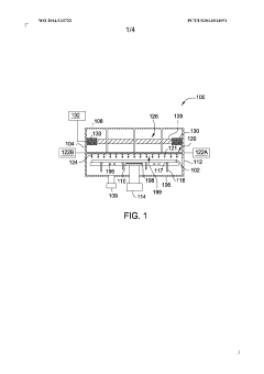
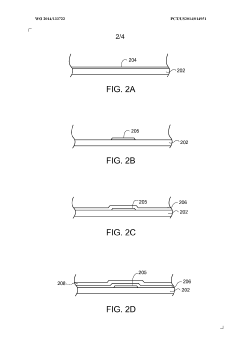
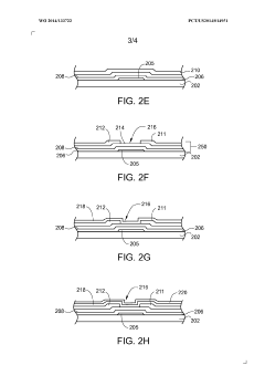
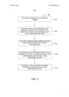
PatentWO2014133722A1
Innovation
- The use of microwave PECVD (MW-PECVD) to deposit hydrogen-free silicon oxyfluoride (SiOF) channel interface layers and subsequent silicon-containing cap layers, reducing hydrogen incorporation and enhancing film stability.
Stability enhancements in metal oxide semiconductor thin film transistors
PatentWO2010074927A2
Innovation
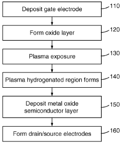
- Exposing the dielectric layer to a hydrogen-containing plasma before depositing the metal oxide semiconductor layer creates a hydrogenated region at the semiconductor-dielectric interface, enhancing carrier mobility and reducing hysteresis, thereby stabilizing the TFTs.
Integration Challenges with Conventional Semiconductors
The integration of Metal Oxide Thin-Film Transistors (TFTs) with conventional semiconductor technologies presents significant technical challenges that must be addressed for successful implementation in advanced semiconductor designs. The fundamental material incompatibility between metal oxide semiconductors and traditional silicon-based technologies creates interface issues that can compromise device performance and reliability. Metal oxide TFTs typically operate at different voltage thresholds compared to conventional CMOS devices, requiring complex level-shifting circuits and specialized power management solutions.
Temperature sensitivity poses another critical challenge, as metal oxide TFTs often exhibit performance degradation at the high processing temperatures used in standard semiconductor fabrication. This necessitates the development of low-temperature processing techniques or thermal isolation strategies to protect metal oxide components during integration. The difference in feature sizes between mature silicon technologies (often at advanced nodes below 10nm) and metal oxide TFTs (typically at much larger dimensions) creates scaling mismatches that complicate circuit design and layout optimization.
Process contamination risks represent a significant concern, as metal elements from oxide TFTs can potentially diffuse into silicon regions, altering electrical characteristics and compromising device functionality. Specialized barrier layers and contamination control protocols must be implemented to mitigate these risks. Additionally, the electrical performance disparities between these technologies—particularly in terms of carrier mobility, switching speed, and noise characteristics—require careful circuit design considerations to ensure optimal system performance.
Manufacturing integration presents practical challenges related to equipment compatibility, process flow modifications, and yield management. Existing semiconductor fabrication lines must be adapted or supplemented with specialized equipment to accommodate the unique requirements of metal oxide TFT production. This often necessitates significant capital investment and process engineering efforts.
The reliability gap between mature silicon technologies and emerging metal oxide TFTs remains substantial, with differences in operational lifetime, stability under electrical stress, and environmental sensitivity. Comprehensive reliability testing and qualification protocols must be developed to ensure that integrated systems meet industry standards for longevity and performance consistency.
Despite these challenges, several promising approaches are emerging to facilitate integration. These include the development of buffer layer technologies, advanced heterogeneous integration techniques, and novel 3D stacking architectures that physically separate different semiconductor technologies while maintaining electrical connectivity. Research into compatible materials systems and process optimization continues to advance, gradually reducing the barriers to effective integration of metal oxide TFTs with conventional semiconductor technologies.
Sustainability and Environmental Impact Assessment
Metal oxide TFTs represent a significant advancement in semiconductor technology that offers substantial environmental benefits compared to conventional silicon-based technologies. The manufacturing processes for metal oxide semiconductors typically require lower processing temperatures (200-300°C) compared to traditional silicon technologies (>1000°C), resulting in significantly reduced energy consumption during production. This temperature difference translates to approximately 30-40% lower carbon footprint in manufacturing facilities.
The materials used in metal oxide TFTs also present environmental advantages. Many metal oxide semiconductors utilize abundant elements such as indium, gallium, zinc, and tin, reducing dependence on scarce resources. Additionally, these materials generally contain fewer toxic components than conventional semiconductor materials, minimizing environmental hazards during both production and disposal phases.
From a lifecycle perspective, devices incorporating metal oxide TFTs demonstrate extended operational lifespans due to their inherent stability. Research indicates that properly engineered metal oxide TFT displays can maintain performance parameters for 10+ years under normal operating conditions, reducing electronic waste generation compared to less durable alternatives.
Power efficiency represents another critical sustainability advantage. Metal oxide TFTs typically require 15-25% less operational power than their silicon counterparts in comparable applications, particularly in display technologies. This efficiency translates to reduced energy consumption throughout the product lifecycle, contributing to lower carbon emissions during the use phase.
Recyclability assessments indicate that metal oxide TFT components can be recovered at rates of 60-75%, though challenges remain in separating the thin-film layers efficiently. Several research initiatives are currently focused on developing improved recycling methodologies specifically for metal oxide semiconductor materials.
Water usage during manufacturing presents a mixed sustainability profile. While some metal oxide deposition techniques require less water than traditional silicon processing, the specialized cleaning procedures may offset these gains. Industry leaders have implemented water recycling systems that reduce consumption by up to 40% in advanced manufacturing facilities.
Looking forward, emerging research in biodegradable substrates compatible with metal oxide TFTs promises to further enhance environmental credentials. These developments could potentially address end-of-life concerns by enabling partially biodegradable electronic components, representing a significant step toward truly sustainable semiconductor technologies.
Unlock deeper insights with Patsnap Eureka Quick Research — get a full tech report to explore trends and direct your research. Try now!
Generate Your Research Report Instantly with AI Agent
Supercharge your innovation with Patsnap Eureka AI Agent Platform!