

Analyzing Resistive RAM's Role in Modern Computing
OCT 9, 20259 MIN READ
Generate Your Research Report Instantly with AI Agent
PatSnap Eureka helps you evaluate technical feasibility & market potential.
ReRAM Technology Background and Objectives
Resistive Random Access Memory (ReRAM) represents a significant evolution in non-volatile memory technology, emerging from decades of research into alternative memory solutions. The technology's foundations can be traced back to the 1960s when researchers first observed resistive switching phenomena in oxide materials. However, it wasn't until the early 2000s that ReRAM began to gain serious attention as a potential successor to conventional memory technologies like NAND flash and DRAM.
The fundamental principle behind ReRAM involves the formation and dissolution of conductive filaments within an insulating dielectric layer, allowing for reversible switching between high and low resistance states. This mechanism enables ReRAM to store binary information in a non-volatile manner, maintaining data even when power is removed from the system.
The evolution of ReRAM technology has been driven by increasing demands for faster, more energy-efficient, and higher-density memory solutions in modern computing systems. Traditional memory technologies face significant scaling challenges as device dimensions approach physical limits, creating a technological gap that ReRAM aims to fill.
Current technological objectives for ReRAM development focus on several key areas. First, improving switching speed to enable ReRAM to compete with DRAM's performance while maintaining non-volatility. Second, enhancing endurance capabilities to support the high write cycles required in both storage and computing applications. Third, reducing power consumption to meet the energy efficiency demands of mobile and edge computing devices.
Another critical objective involves addressing reliability issues, particularly the variability in switching behavior and retention characteristics that can affect long-term data stability. Researchers are exploring various material compositions and device architectures to optimize these parameters.
The integration of ReRAM into existing semiconductor manufacturing processes represents another significant goal. Compatibility with CMOS technology is essential for cost-effective production and widespread adoption in commercial applications.
Beyond traditional memory applications, ReRAM technology shows promise for neuromorphic computing implementations. Its analog switching characteristics closely resemble biological synaptic behavior, making it an attractive candidate for hardware-based neural networks and brain-inspired computing architectures.
The trajectory of ReRAM development indicates a shift from purely memory-centric applications toward computational memory paradigms, where data processing occurs within the memory itself. This in-memory computing approach aims to overcome the von Neumann bottleneck that limits conventional computing architectures, potentially enabling significant improvements in energy efficiency and performance for data-intensive applications.
Market Demand Analysis for Non-Volatile Memory
The non-volatile memory (NVM) market has experienced significant growth in recent years, driven by increasing demand for data storage solutions across various sectors. The global NVM market was valued at approximately $67 billion in 2022 and is projected to reach $125 billion by 2028, representing a compound annual growth rate (CAGR) of around 11%. This growth trajectory underscores the expanding role of NVM technologies, particularly Resistive RAM (ReRAM), in modern computing architectures.
The primary market drivers for NVM technologies include the explosive growth in data generation, with global data creation projected to exceed 180 zettabytes by 2025. This data deluge necessitates storage solutions that combine high density, low power consumption, and non-volatility – characteristics that ReRAM potentially offers. Additionally, the proliferation of Internet of Things (IoT) devices, expected to surpass 75 billion connected devices by 2025, creates substantial demand for embedded memory solutions with minimal power requirements.
Enterprise data centers represent another significant market segment, with spending on data center infrastructure reaching $200 billion annually. These facilities increasingly require high-performance, energy-efficient memory solutions to handle massive data processing workloads while minimizing operational costs. ReRAM's potential for high-density storage with lower power consumption positions it as a promising candidate for next-generation data center architectures.
The automotive sector presents an emerging market opportunity for NVM technologies, particularly with the rise of autonomous vehicles. Advanced driver-assistance systems (ADAS) and autonomous driving platforms require robust, high-endurance memory solutions capable of operating in harsh environmental conditions. The automotive memory market is expected to grow at a CAGR of 23% through 2026, reaching $12 billion.
Consumer electronics continues to be a major market driver for NVM technologies. The smartphone market alone, with annual shipments exceeding 1.3 billion units, creates substantial demand for high-performance, energy-efficient memory solutions. ReRAM's potential for faster write speeds and lower power consumption compared to traditional flash memory makes it particularly attractive for mobile applications.
Edge computing applications represent another growth vector for NVM technologies. As computational workloads increasingly shift toward the network edge, the demand for memory solutions that combine performance, energy efficiency, and reliability continues to rise. The edge computing market is projected to reach $43 billion by 2027, creating significant opportunities for innovative memory technologies like ReRAM.
Despite these promising market indicators, challenges remain in terms of manufacturing scalability, cost competitiveness with established technologies like NAND flash, and ecosystem development. The path to widespread commercial adoption will require addressing these barriers while demonstrating compelling performance and economic advantages over incumbent solutions.
ReRAM Development Status and Technical Challenges
Resistive RAM (ReRAM) technology has emerged as a promising non-volatile memory solution, yet its widespread adoption faces several significant technical challenges. Currently, ReRAM development has reached a stage where laboratory demonstrations have proven its theoretical advantages, including high density, low power consumption, and fast switching speeds. However, the transition from laboratory to mass production remains problematic due to reliability and scalability issues.
The global landscape of ReRAM development shows concentrated research efforts in the United States, Japan, South Korea, and China. Companies like Crossbar, Weebit Nano, and TSMC have made substantial progress, while research institutions such as Stanford University and IMEC continue to push theoretical boundaries. This geographical distribution reflects both commercial interests and national strategic priorities in advanced semiconductor technologies.
A primary technical challenge for ReRAM is endurance limitation. Current ReRAM cells typically achieve 10^6 to 10^9 write cycles, which falls short of DRAM's capabilities and remains insufficient for certain high-intensity computing applications. The physical mechanisms behind resistance switching degradation, including oxygen vacancy migration and filament formation instability, require further fundamental research to overcome these limitations.
Variability presents another significant hurdle. ReRAM cells exhibit considerable device-to-device and cycle-to-cycle variations in resistance states, switching voltages, and retention characteristics. This inconsistency complicates the design of reliable sensing circuits and error correction mechanisms, ultimately affecting yield rates in manufacturing processes.
The scaling challenge cannot be overlooked. While ReRAM theoretically offers excellent scaling potential down to sub-10nm nodes, practical implementation encounters issues with current leakage, crosstalk between adjacent cells, and maintaining adequate signal-to-noise ratios at reduced dimensions. These factors potentially limit the density advantages that make ReRAM attractive as a storage solution.
Material science constraints further complicate ReRAM development. The complex oxide materials commonly used in ReRAM structures, such as HfOx, TaOx, and TiOx, present integration challenges with conventional CMOS processes. Controlling the stoichiometry, crystallinity, and interface properties of these materials at industrial scale remains difficult, affecting device performance consistency.
Power consumption optimization represents another critical challenge. Although ReRAM offers lower operational power than flash memory, the SET/RESET operations still require relatively high current densities that can cause thermal issues in high-density arrays. Reducing the switching current while maintaining reliable operation presents a fundamental trade-off that researchers continue to address through novel materials and cell architectures.
Current ReRAM Implementation Solutions
01 ReRAM device structures and fabrication methods
Various device structures and fabrication methods for Resistive RAM (ReRAM) have been developed to enhance performance and reliability. These include specific electrode materials, resistive switching layers, and novel integration approaches. The fabrication processes often involve deposition techniques such as atomic layer deposition, sputtering, or chemical vapor deposition to create the multi-layer structure required for ReRAM operation. These structures typically consist of a top electrode, resistive switching layer, and bottom electrode configured to enable reliable resistive switching behavior.- ReRAM device structures and fabrication methods: Resistive Random Access Memory (ReRAM) devices can be fabricated using various structures and methods to enhance performance and reliability. These include multi-layer stacks with specific electrode materials, resistive switching layers, and barrier layers. Advanced fabrication techniques such as atomic layer deposition and specialized etching processes are employed to create precise device structures with controlled interfaces, which are critical for consistent switching behavior and long-term stability.
- ReRAM switching mechanisms and materials: The resistive switching mechanism in ReRAM is based on the formation and rupture of conductive filaments within a resistive switching layer. Various materials are used for this layer, including metal oxides (HfOx, TaOx), chalcogenides, and perovskites. The selection of materials affects key performance parameters such as switching speed, endurance, retention time, and power consumption. Doping strategies and interface engineering are employed to optimize the switching behavior and reliability of ReRAM devices.
- ReRAM array architecture and integration: ReRAM arrays can be implemented in various architectures including crossbar arrays, 3D stacked structures, and hybrid configurations. Integration challenges include sneak path current mitigation, selector device implementation, and compatibility with CMOS processes. Advanced array designs incorporate selector devices such as transistors or diodes to enable precise cell addressing and minimize interference between adjacent cells. These architectures aim to maximize density while maintaining reliable operation and addressing capabilities.
- ReRAM for neuromorphic computing applications: ReRAM devices are increasingly being utilized for neuromorphic computing applications due to their ability to mimic synaptic behavior. The analog resistance states of ReRAM can represent synaptic weights in artificial neural networks, enabling efficient implementation of learning algorithms. Specialized ReRAM designs for neuromorphic applications focus on achieving linear and symmetric conductance changes, multi-level states, and low power operation. These characteristics make ReRAM promising for edge AI applications and brain-inspired computing systems.
- ReRAM reliability and performance optimization: Enhancing the reliability and performance of ReRAM involves addressing challenges such as resistance drift, endurance limitations, and variability between cells. Techniques include optimized programming schemes, error correction methods, and specialized circuit designs for read/write operations. Temperature compensation techniques and reference cell designs are implemented to ensure stable operation across varying environmental conditions. Advanced characterization methods are used to understand failure mechanisms and develop strategies to extend device lifetime and improve overall performance metrics.
02 Resistive switching materials and mechanisms
The core functionality of ReRAM depends on resistive switching materials and their underlying mechanisms. Various materials including metal oxides, chalcogenides, and organic compounds exhibit resistive switching behavior through mechanisms such as filament formation/rupture, interface effects, or phase changes. The selection of appropriate materials and understanding their switching mechanisms are crucial for controlling parameters like switching voltage, retention time, endurance, and power consumption. These materials can be engineered at the nanoscale to optimize the formation and dissolution of conductive filaments.Expand Specific Solutions03 ReRAM array architecture and integration
ReRAM array architectures are designed to maximize density, minimize cross-talk, and enable efficient addressing of individual memory cells. Various integration schemes include crossbar arrays, 3D stacking, and hybrid integration with CMOS technology. These architectures address challenges such as sneak path currents, which can cause read errors in high-density arrays. Advanced selector devices or transistors are often incorporated to isolate individual cells during read and write operations, enabling higher density memory arrays while maintaining reliable operation.Expand Specific Solutions04 Programming and operation methods for ReRAM
Specific programming and operation methods have been developed to control the resistive switching process in ReRAM devices. These include pulse width modulation, current compliance techniques, and multi-level cell programming approaches. The programming methods aim to achieve reliable switching between high and low resistance states while minimizing variability and extending device lifetime. Advanced read schemes are also implemented to accurately detect the resistance state while minimizing disturbance to neighboring cells, enabling more reliable data storage and retrieval.Expand Specific Solutions05 Applications and integration with other technologies
ReRAM technology has been integrated with various other technologies for specialized applications beyond conventional memory storage. These include neuromorphic computing, in-memory computing, and edge AI applications that leverage the analog nature of resistive switching. ReRAM cells can be configured to mimic synaptic behavior for neural network implementations or combined with sensors for edge computing applications. The non-volatile nature and low power consumption of ReRAM make it particularly suitable for Internet of Things (IoT) devices and other energy-constrained applications requiring persistent memory.Expand Specific Solutions
Key Industry Players in ReRAM Development
Resistive RAM (ReRAM) technology is emerging as a significant player in modern computing, currently positioned in the early growth phase of its industry development. The global ReRAM market, though still relatively small compared to traditional memory technologies, is projected to expand rapidly due to increasing demand for high-performance, low-power memory solutions in IoT, AI, and edge computing applications. From a technical maturity perspective, companies like Micron Technology, Crossbar, and KIOXIA are leading commercial development, while IBM, SK hynix, and Taiwan Semiconductor Manufacturing Co. are advancing fundamental research. Traditional memory manufacturers including Winbond Electronics and Macronix are also pivoting toward ReRAM technology. University collaborations with Fudan University and University of Michigan are accelerating innovation, indicating ReRAM is transitioning from research to early commercialization, with significant growth potential as manufacturing processes mature.
Micron Technology, Inc.
Technical Solution: Micron has developed 3D XPoint™ technology (in collaboration with Intel) and is advancing proprietary ReRAM solutions. Their approach utilizes a chalcogenide-based material system with selector devices to enable high-density crosspoint arrays. Micron's ReRAM technology demonstrates switching speeds in the nanosecond range, with endurance capabilities exceeding 10^9 cycles [4]. The company has integrated their ReRAM technology with advanced process nodes, achieving cell sizes below 10nm. Micron's implementation focuses on storage class memory applications, positioning ReRAM as an intermediate layer between DRAM and NAND flash in the memory hierarchy. Their technology enables bit-addressable operations with byte-level write capabilities, unlike traditional flash memory that requires block-level operations [5]. Micron has also explored ReRAM for in-memory computing applications, leveraging the analog nature of resistive switching for efficient matrix operations in AI workloads [6].
Strengths: Established manufacturing infrastructure; integration with existing memory ecosystem; strong IP portfolio; byte-addressable architecture; potential for storage class memory applications. Weaknesses: Higher cost per bit compared to NAND flash; thermal stability challenges at advanced nodes; variability in resistance states requiring sophisticated error correction.
International Business Machines Corp.
Technical Solution: IBM has pioneered Phase Change Memory (PCM), a specific type of ReRAM, with their research focusing on multi-level cell capabilities and reliability enhancement. IBM's PCM technology utilizes germanium antimony telluride (GST) materials that change between amorphous and crystalline states to represent different resistance levels. Their implementation has achieved 3 bits per cell, significantly increasing storage density [7]. IBM has demonstrated PCM arrays with access times of less than 100ns and endurance exceeding 10^6 cycles. The company has integrated their ReRAM technology with conventional CMOS processes, enabling hybrid computing architectures. IBM's research has extended to neuromorphic computing applications, where ReRAM arrays function as artificial synapses in neural network implementations, achieving significant energy efficiency improvements compared to conventional computing approaches [8]. Their technology has demonstrated analog weight updates suitable for on-chip training of neural networks [9].
Strengths: Advanced multi-level cell capability; strong research foundation; integration with neuromorphic computing; established reliability engineering expertise; compatibility with standard semiconductor processes. Weaknesses: Complex programming schemes required for multi-level operation; drift in resistance states over time; temperature sensitivity affecting long-term stability.
Critical ReRAM Patents and Technical Innovations
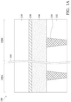
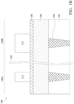
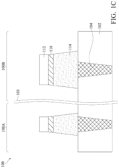
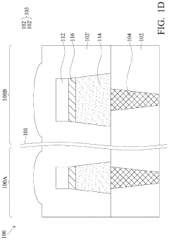
Resistive random access memory
PatentActiveUS20170330915A1
Innovation
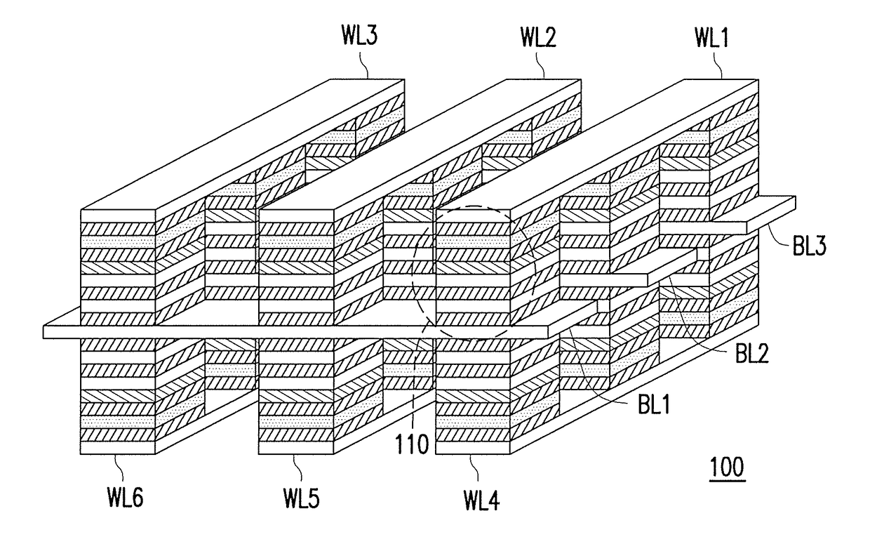
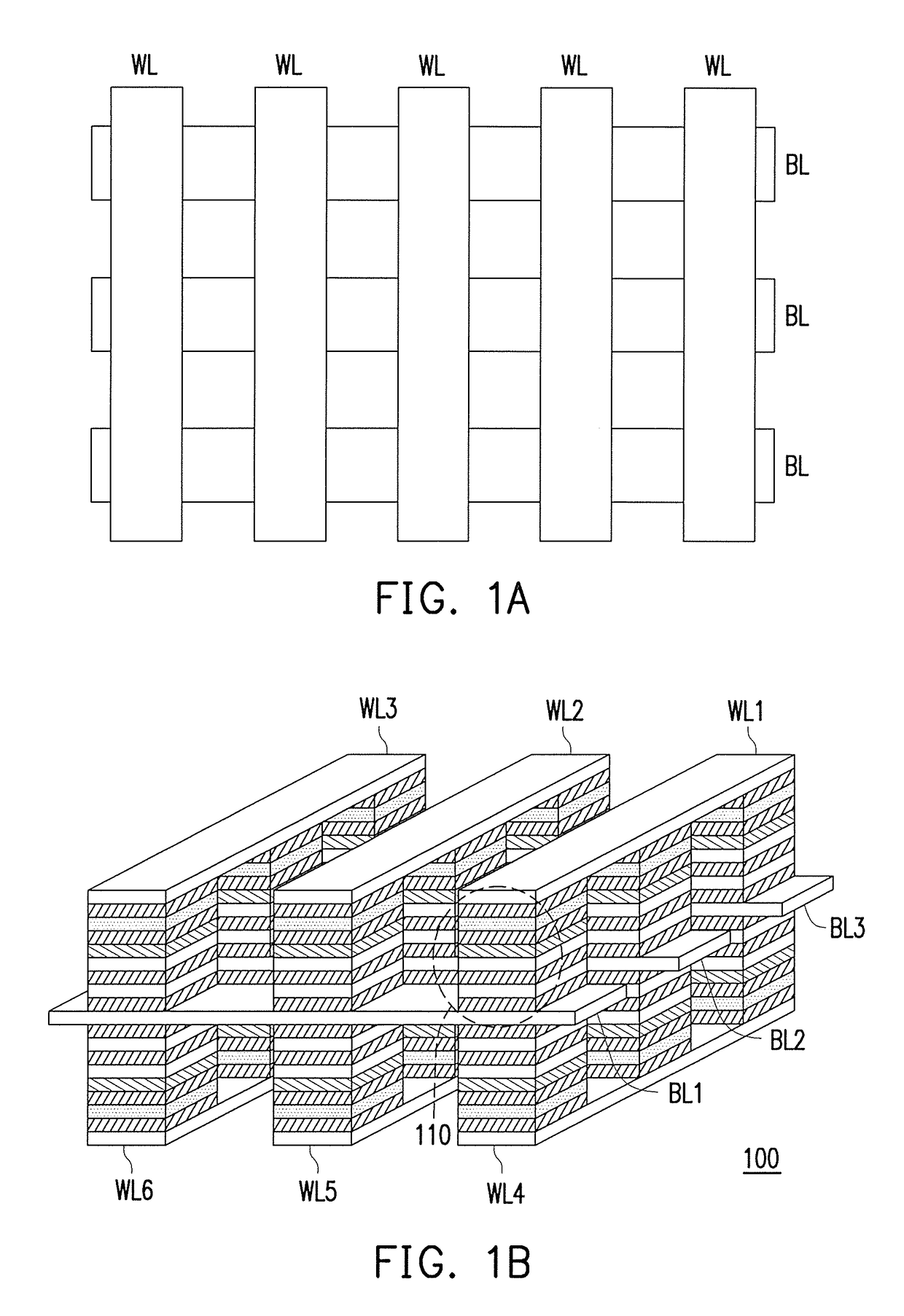
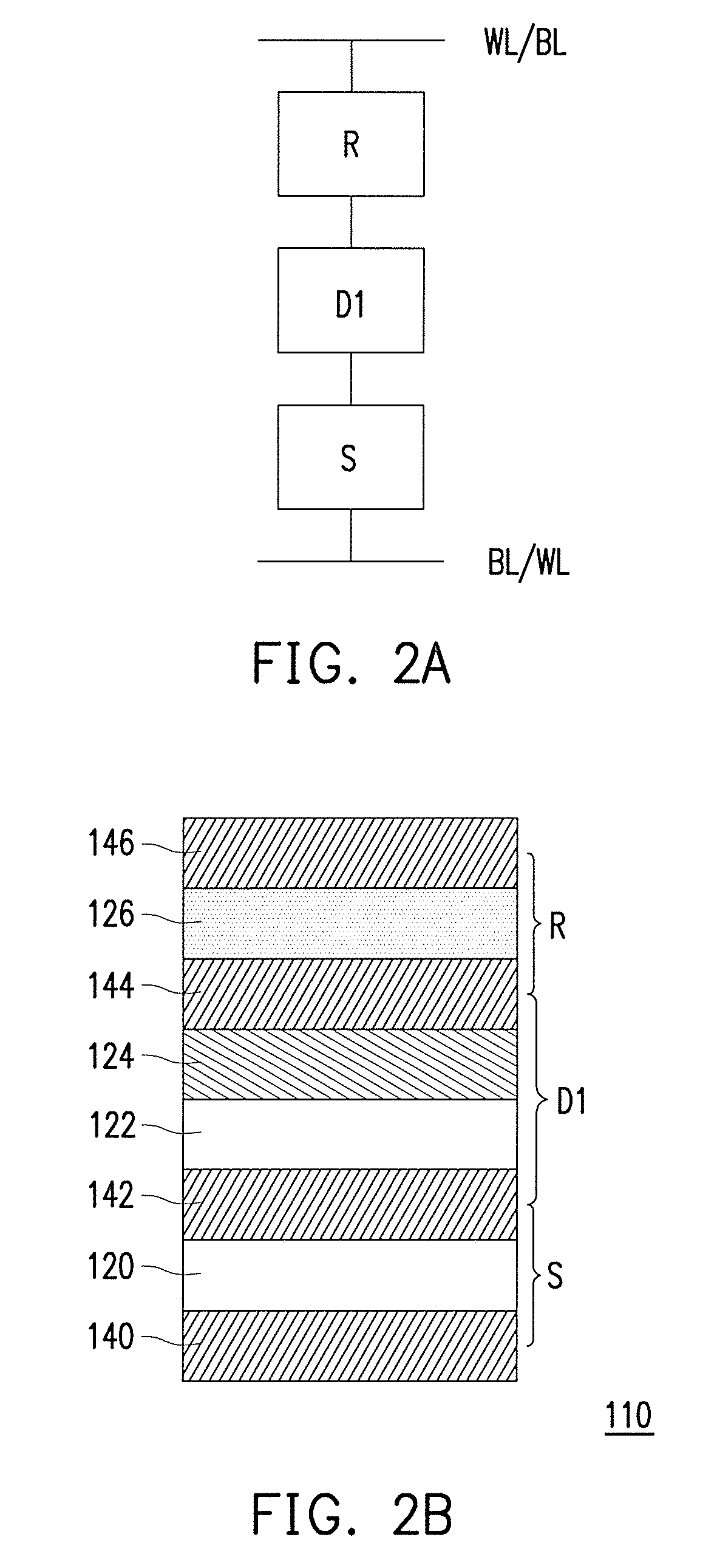
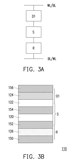
- The resistive random access memory device is designed with a memory cell structure that includes a selector structure, a current limiter structure, and a resistor structure in series, using specific conductive and material layers to reduce dimensions and enhance integration, replacing the traditional 1T1R structure with a 1R1D or 1D1S structure.
Resistive random access memory and method for manufacturing the same
PatentActiveUS20230225228A1
Innovation
- A direct contact configuration between the conductive line structure and the memory unit is established, eliminating the need for vias and reducing series resistance, which involves forming a conductive line structure with a lower electrode directly on its surface, followed by a resistive switching layer and an upper electrode, thereby simplifying the manufacturing process and reducing costs.
Energy Efficiency Comparison with Traditional Memory
Resistive RAM (ReRAM) demonstrates significant energy efficiency advantages over traditional memory technologies, positioning it as a promising solution for next-generation computing systems. When comparing power consumption metrics, ReRAM operates at approximately 10-100 times lower energy per bit operation than conventional DRAM. This dramatic reduction stems from ReRAM's fundamental operating principle - it doesn't require constant power refreshing to maintain stored data, unlike DRAM which necessitates periodic charge replenishment.
The standby power consumption of ReRAM systems is particularly impressive, with measurements showing up to 95% reduction compared to equivalent DRAM configurations in idle states. This characteristic makes ReRAM especially valuable for edge computing devices and IoT applications where battery life and thermal management are critical constraints.
Write operations in ReRAM consume approximately 0.1-1 pJ per bit, compared to DRAM's 10-20 pJ per bit. This order-of-magnitude improvement translates directly to reduced system-level power requirements. Similarly, read operations demonstrate 3-5x better energy efficiency in ReRAM implementations versus traditional memory technologies.
Beyond direct operational energy savings, ReRAM's non-volatile nature eliminates the need for energy-intensive data transfers between volatile memory and storage systems. In conventional computing architectures, significant energy is expended moving data between DRAM and storage media like SSDs or HDDs. ReRAM's persistence capability enables in-memory computing paradigms that substantially reduce these data movement costs, which can account for up to 60% of total system energy in data-intensive applications.
Temperature sensitivity also factors into energy efficiency considerations. ReRAM maintains stable performance across a wider temperature range than DRAM, reducing cooling requirements in data centers and high-performance computing environments. Studies indicate potential cooling energy savings of 15-25% in large-scale deployments.
When evaluated in real-world workloads, ReRAM-based systems have demonstrated 30-70% total energy reduction depending on application characteristics. Data-intensive tasks with frequent memory access patterns show the most dramatic improvements, while compute-bound workloads see more modest but still significant gains.
The manufacturing energy footprint of ReRAM is also becoming increasingly competitive as production scales. While early fabrication processes required more energy than established DRAM manufacturing, recent advancements in materials science and production techniques have narrowed this gap considerably, promising further improvements in lifecycle energy efficiency.
Integration Challenges with Existing Computing Architectures
The integration of Resistive RAM (ReRAM) into existing computing architectures presents significant challenges that must be addressed before widespread adoption can occur. Current computing systems are built around the von Neumann architecture, which separates processing and memory units, creating the well-known "memory wall" bottleneck. ReRAM, as an emerging non-volatile memory technology, requires fundamental changes to this established paradigm to fully leverage its potential.
One primary challenge is the interface compatibility between ReRAM arrays and conventional CMOS technology. While ReRAM cells can be fabricated using materials compatible with CMOS processes, the integration of these two technologies requires careful consideration of signal levels, timing requirements, and power management. The voltage levels required for ReRAM operations often differ from standard CMOS logic levels, necessitating specialized interface circuits that can bridge this gap efficiently.
Thermal management presents another significant hurdle. ReRAM programming operations, particularly SET and RESET processes, generate considerable heat that can affect nearby components and potentially degrade the reliability of both the ReRAM cells and surrounding circuitry. This thermal concern becomes especially critical in high-density implementations where cells are packed closely together.
The endurance limitations of current ReRAM technologies also pose integration challenges. While significantly better than flash memory, ReRAM cells typically support 10^6 to 10^9 write cycles, which falls short of SRAM and DRAM capabilities. This disparity requires sophisticated wear-leveling algorithms and error correction mechanisms to ensure system reliability over time, adding complexity to memory controllers and system software.
From an architectural perspective, effectively utilizing ReRAM's unique characteristics demands new memory hierarchies and data movement strategies. Traditional cache coherence protocols and memory access patterns are optimized for volatile memories with uniform access times, whereas ReRAM exhibits asymmetric read/write latencies and non-volatility. This mismatch necessitates rethinking how data flows between processing units and memory subsystems.
The lack of standardized interfaces and protocols specifically designed for ReRAM integration further complicates adoption. Current memory interfaces like DDR and LPDDR are optimized for DRAM characteristics and may not efficiently accommodate ReRAM's operational parameters. Industry-wide standards for ReRAM integration would accelerate adoption but remain in early development stages.
Power management systems in existing architectures also require adaptation to handle ReRAM's unique power profile. While ReRAM offers excellent power efficiency during idle states due to its non-volatility, its write operations can demand significant current spikes that existing power delivery networks may not be designed to handle efficiently.
Unlock deeper insights with PatSnap Eureka Quick Research — get a full tech report to explore trends and direct your research. Try now!
Generate Your Research Report Instantly with AI Agent
Supercharge your innovation with PatSnap Eureka AI Agent Platform!