

Atomic Force Microscopy Vs X-Ray Diffraction: Application Insights
SEP 19, 20259 MIN READ
Generate Your Research Report Instantly with AI Agent
PatSnap Eureka helps you evaluate technical feasibility & market potential.
AFM and XRD Technology Background and Objectives
Atomic Force Microscopy (AFM) and X-Ray Diffraction (XRD) represent two cornerstone analytical techniques in materials science and nanotechnology. Since their inception, these technologies have evolved along distinct yet complementary paths, each offering unique insights into material properties at different scales and dimensions.
AFM emerged in the 1980s as an extension of Scanning Tunneling Microscopy, pioneered by Gerd Binnig and Heinrich Rohrer. The breakthrough came in 1986 when Binnig, Quate, and Gerber developed the first AFM, enabling researchers to visualize surfaces at the nanoscale with unprecedented resolution. Over subsequent decades, AFM technology has progressed from basic topographical imaging to advanced modes including force spectroscopy, electrical characterization, and biological applications in liquid environments.
XRD, conversely, has a longer historical trajectory dating back to Max von Laue's discovery of X-ray diffraction by crystals in 1912, followed by the seminal work of William Henry Bragg and William Lawrence Bragg. This technique has evolved from rudimentary film-based detection systems to sophisticated digital detectors with enhanced sensitivity and resolution, enabling increasingly precise structural determinations.
The technological objectives for both AFM and XRD continue to evolve in response to emerging scientific challenges. For AFM, current development goals include improving temporal resolution for real-time imaging of dynamic processes, enhancing force sensitivity for single-molecule studies, and expanding multimodal capabilities to simultaneously capture various physical properties. Integration with complementary techniques and automation for high-throughput analysis represent additional frontiers.
XRD technology aims to achieve higher spatial resolution for heterogeneous samples, reduced acquisition times for time-resolved studies, and enhanced sensitivity for trace phase detection. The miniaturization of XRD systems for portable applications and the development of non-destructive in-situ measurement capabilities are also significant objectives in the field.
The convergence of these technologies presents intriguing possibilities. Correlative approaches combining AFM's surface sensitivity with XRD's bulk structural insights offer comprehensive material characterization across multiple length scales. This synergistic approach addresses the limitations inherent to each individual technique, providing researchers with more complete understanding of complex material systems.
As materials science advances toward increasingly complex nanomaterials, quantum materials, and biological systems, the continued evolution of AFM and XRD technologies remains crucial. Their complementary capabilities in probing structural and functional properties position them as indispensable tools in the scientific arsenal for addressing challenges in energy storage, semiconductor technology, pharmaceutical development, and beyond.
Market Applications and Demand Analysis
The market for advanced analytical instrumentation continues to expand, driven by increasing demands across multiple sectors including materials science, semiconductor manufacturing, pharmaceuticals, and nanotechnology. Atomic Force Microscopy (AFM) and X-Ray Diffraction (XRD) represent two distinct yet complementary technologies that serve critical roles in these markets, with each addressing specific analytical needs.
The global market for AFM equipment was valued at approximately $570 million in 2022 and is projected to grow at a compound annual growth rate of 6.8% through 2030. This growth is primarily fueled by increasing applications in nanomaterials research, biological sciences, and semiconductor quality control. The demand for high-resolution surface imaging at the nanoscale continues to drive AFM adoption, particularly in research institutions and advanced manufacturing facilities.
In contrast, the XRD market reached about $1.6 billion in 2022, with forecasts indicating growth at 5.4% annually through 2030. XRD technology benefits from its established position in crystallography and materials characterization, with strong demand from pharmaceutical companies for drug development and quality control, as well as from metallurgical industries for structural analysis of alloys and composites.
Regional analysis reveals that North America and Europe currently dominate the market for both technologies, accounting for over 60% of global installations. However, the Asia-Pacific region, particularly China, Japan, and South Korea, is experiencing the fastest growth rates due to expanding semiconductor manufacturing capabilities and increasing investments in research infrastructure.
Industry-specific demand patterns show distinct preferences between the two technologies. Semiconductor manufacturers increasingly rely on AFM for process control and defect analysis at sub-nanometer resolutions. Meanwhile, pharmaceutical companies favor XRD for polymorph screening and crystallinity assessment in drug formulation processes. The materials science sector utilizes both technologies extensively, with selection typically depending on specific research requirements.
Recent market surveys indicate that end-users are increasingly seeking integrated analytical solutions that combine multiple characterization techniques. This trend has prompted instrument manufacturers to develop platforms that offer complementary capabilities or seamless data integration between AFM and XRD systems, addressing the growing demand for comprehensive material characterization workflows.
The academic research sector remains a significant market driver for both technologies, accounting for approximately 40% of new instrument acquisitions. However, industrial applications are growing at a faster rate, particularly in quality control and failure analysis applications where rapid, non-destructive testing capabilities are essential for maintaining production efficiency.
Current Technological Status and Challenges
Atomic Force Microscopy (AFM) and X-Ray Diffraction (XRD) represent two distinct yet complementary analytical techniques that have revolutionized materials characterization across multiple scientific disciplines. Currently, both technologies have reached significant maturity, with AFM evolving from its invention in the 1980s to become a versatile nanoscale imaging tool, while XRD has been refined over a century into a standard method for crystallographic analysis.
The global market for these technologies continues to expand, with the AFM market valued at approximately $570 million and growing at a CAGR of 6.5%, while the XRD equipment market exceeds $1.5 billion with a 5.8% growth rate. This expansion reflects their increasing adoption across semiconductor, pharmaceutical, and advanced materials industries.
Despite their widespread application, both technologies face substantial challenges. AFM encounters limitations in scanning speed, with typical high-resolution scans requiring minutes to hours, creating bottlenecks in high-throughput research environments. Additionally, AFM tip degradation during operation affects measurement reliability and necessitates frequent replacement, increasing operational costs and reducing productivity.
XRD systems, while powerful for crystalline materials analysis, struggle with amorphous samples and nanomaterials with limited long-range order. The technique also requires relatively large sample volumes compared to surface-sensitive methods, limiting its application in nanoscale material development where sample quantities are often restricted.
Geographically, these technologies show distinct distribution patterns. North America and Europe dominate the high-end AFM market, with approximately 65% of advanced research instruments, while Asia-Pacific leads in production volume of standard AFM systems. For XRD, Japan and Germany maintain technological leadership in instrument development, though China has emerged as the fastest-growing market for both technologies, driven by substantial investments in semiconductor and materials research infrastructure.
Integration challenges persist between these complementary techniques. While AFM provides exceptional surface topography information and XRD delivers crystallographic structure data, researchers often struggle to correlate findings between the two methods due to differences in sampling volumes, resolution capabilities, and data formats. This has prompted recent development of hybrid systems and correlative microscopy approaches, though standardized workflows remain elusive.
Environmental sensitivity presents another significant challenge, with both techniques requiring controlled conditions for optimal performance. AFM particularly suffers from environmental vibrations and temperature fluctuations, while XRD accuracy can be compromised by sample preparation inconsistencies and preferred orientation effects.
Comparative Analysis of AFM and XRD Methodologies
01 Combined AFM and XRD for material characterization
The integration of Atomic Force Microscopy (AFM) and X-Ray Diffraction (XRD) techniques provides complementary data for comprehensive material characterization. AFM offers high-resolution surface topography and mechanical properties at the nanoscale, while XRD provides crystallographic information about the bulk material. This combination allows researchers to correlate surface features with crystalline structure, enabling more complete analysis of materials such as thin films, nanostructures, and crystalline samples.- Combined AFM and XRD for material characterization: The integration of Atomic Force Microscopy (AFM) and X-Ray Diffraction (XRD) techniques provides complementary data for comprehensive material characterization. AFM offers high-resolution surface topography and mechanical properties at the nanoscale, while XRD provides crystallographic information about the bulk material. This combination allows researchers to correlate surface morphology with crystal structure, enabling more complete analysis of materials such as thin films, nanostructures, and crystalline materials.
- Instrumentation advancements for combined AFM-XRD measurements: Specialized instrumentation has been developed to enable simultaneous or sequential AFM and XRD measurements on the same sample area. These systems incorporate precise positioning mechanisms, environmental controls, and integrated data acquisition systems. Advanced designs allow for in-situ measurements under various conditions such as controlled temperature, pressure, or chemical environments, facilitating real-time observation of material transformations and reactions at multiple length scales.
- Analysis of thin films and surface structures: AFM and XRD techniques are particularly valuable for analyzing thin films and surface structures. AFM provides detailed information about surface roughness, grain boundaries, and defects, while XRD techniques such as grazing incidence XRD can determine crystalline phases, orientation, and strain in thin films. This combined approach enables researchers to understand growth mechanisms, interface properties, and structural evolution in layered materials, semiconductor devices, and functional coatings.
- Nanomechanical and structural property correlation: The combination of AFM and XRD enables correlation between nanomechanical properties and crystallographic structure. AFM modes such as force spectroscopy, nanoindentation, and friction measurements provide mechanical property data, while XRD reveals crystal structure, phase composition, and lattice parameters. This correlation helps in understanding structure-property relationships in materials, allowing for the development of materials with tailored mechanical properties for specific applications.
- Data processing and analysis methods: Advanced data processing and analysis methods have been developed to extract meaningful information from combined AFM and XRD measurements. These include multivariate statistical analysis, machine learning algorithms, and computational modeling approaches that integrate data from both techniques. Such methods enable automated feature recognition, quantitative analysis of crystallinity, defect identification, and correlation of structural features across different length scales, enhancing the efficiency and accuracy of material characterization.
02 AFM and XRD instrumentation advancements
Technological advancements in instrumentation have enabled the integration of Atomic Force Microscopy and X-Ray Diffraction capabilities into more efficient and precise systems. These innovations include improved probe designs, enhanced detection systems, and specialized sample holders that allow for simultaneous or sequential measurements. Such advancements have led to higher resolution imaging, more accurate crystallographic data, and the ability to perform in-situ measurements under various environmental conditions.Expand Specific Solutions03 Applications in semiconductor and thin film analysis
Atomic Force Microscopy and X-Ray Diffraction are extensively used in semiconductor and thin film analysis to evaluate critical parameters such as surface roughness, crystallinity, strain, and defect density. These techniques help in quality control during manufacturing processes, failure analysis, and research and development of new materials. The combination provides insights into how surface morphology correlates with crystalline structure, which is crucial for optimizing electronic device performance and reliability.Expand Specific Solutions04 Nanomechanical and structural property measurement
The combination of Atomic Force Microscopy and X-Ray Diffraction enables comprehensive characterization of nanomechanical and structural properties of materials. AFM provides direct measurements of mechanical properties such as elasticity, hardness, and adhesion at the nanoscale, while XRD offers information about crystal structure, phase composition, and lattice parameters. Together, these techniques allow researchers to establish relationships between mechanical behavior and underlying crystalline structure, which is valuable for materials engineering and design.Expand Specific Solutions05 Data processing and analysis methods
Advanced data processing and analysis methods have been developed to extract meaningful information from combined Atomic Force Microscopy and X-Ray Diffraction measurements. These methods include correlation algorithms, multivariate statistical analysis, and machine learning approaches that help identify patterns and relationships between surface topography and crystallographic data. Software tools enable the visualization of complex datasets, automated feature recognition, and quantitative analysis of structural and mechanical properties across different length scales.Expand Specific Solutions
Leading Manufacturers and Research Institutions
The Atomic Force Microscopy (AFM) versus X-Ray Diffraction (XRD) market represents a mature yet evolving technological landscape within materials characterization. Currently in a growth phase, this market is estimated at approximately $3-4 billion globally, with steady annual expansion of 5-7%. Leading players include established instrumentation companies like Bruker Nano, Rigaku, and JEOL, alongside diversified technology corporations such as IBM and Hitachi. Academic and research institutions including CNRS, Fraunhofer-Gesellschaft, and various universities contribute significantly to technological advancement. The competitive landscape features clear segmentation between high-precision research instruments and more accessible industrial applications, with recent innovations focusing on hybrid systems and automation. Companies are increasingly developing integrated solutions combining both technologies to address complex characterization challenges across materials science, semiconductor, and life sciences sectors.
Bruker Nano, Inc.
Technical Solution: Bruker Nano has developed comprehensive solutions integrating Atomic Force Microscopy (AFM) and X-Ray Diffraction (XRD) technologies. Their PeakForce Tapping technology enables high-resolution imaging with precise force control, allowing researchers to simultaneously obtain topographical, mechanical, and electrical property measurements at the nanoscale. For materials characterization, Bruker's D8 DISCOVER XRD platform offers advanced crystallographic analysis with capabilities for thin film analysis, texture analysis, and high-resolution reciprocal space mapping. Their innovative approach combines these complementary techniques through correlative microscopy workflows, enabling researchers to analyze the same sample region with both AFM and XRD. This provides multiscale characterization from atomic structure (XRD) to surface topography and properties (AFM), particularly valuable for semiconductor, pharmaceutical, and advanced materials research where understanding structure-property relationships is crucial.
Strengths: Bruker's integrated solutions offer comprehensive characterization across multiple length scales, providing correlative data that neither technique alone could deliver. Their PeakForce Tapping technology significantly reduces sample damage during AFM imaging. Weaknesses: The high cost of their integrated systems limits accessibility for smaller research institutions, and the complexity of operating both techniques requires specialized training and expertise.
International Business Machines Corp.
Technical Solution: IBM has pioneered advanced applications combining Atomic Force Microscopy (AFM) and X-Ray Diffraction (XRD) for semiconductor and quantum computing materials research. Their proprietary AFM technology achieves sub-nanometer resolution imaging with specialized probes for electrical, magnetic, and mechanical property mapping at atomic scales. IBM's approach integrates machine learning algorithms to correlate AFM surface measurements with XRD crystallographic data, enabling predictive modeling of material performance. For semiconductor applications, they've developed in-line metrology systems combining AFM's surface sensitivity with XRD's ability to characterize buried interfaces and strain distributions in advanced node technologies. Their research facilities utilize synchrotron-based XRD techniques alongside custom-built AFM systems for investigating quantum materials, superconductors, and next-generation computing architectures. This integrated approach has been crucial for IBM's development of increasingly miniaturized transistor architectures and novel quantum computing materials.
Strengths: IBM's integration of machine learning with AFM/XRD data analysis enables predictive materials engineering and faster development cycles. Their specialized probe technologies allow characterization of electrical and magnetic properties at unprecedented resolution. Weaknesses: Their solutions are highly customized for semiconductor and quantum computing applications, limiting broader applicability. The systems require significant infrastructure investment and specialized expertise to operate effectively.
Key Technical Innovations and Patents
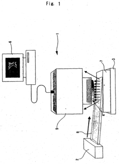
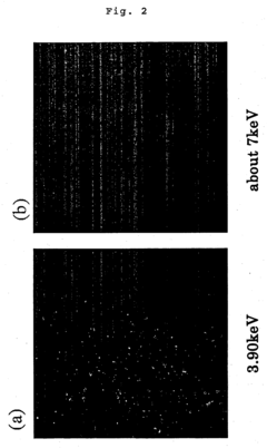
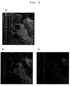
X-ray diffraction microscope and x-ray diffraction measurement method using x-ray diffraction microscope
PatentInactiveEP1672361B1
Innovation
- An X-ray diffraction microscope apparatus utilizing a two-dimensional X-ray detector with energy resolving power, a capillary collimator to suppress angle divergence, and image processing to acquire images in a short time, allowing for imaging of diffracted X-rays without moving the sample or detector, using continuous X-rays and removing high-energy components to enhance resolving power.
Sample Preparation Requirements and Limitations
Sample preparation represents a critical factor in determining the effectiveness and accuracy of both Atomic Force Microscopy (AFM) and X-Ray Diffraction (XRD) techniques. These methodologies impose distinct requirements on sample preparation, which significantly influence their applicability across various research domains.
AFM sample preparation demands meticulous attention to surface cleanliness and smoothness. Samples must typically exhibit surface roughness below 10 nanometers to achieve optimal imaging results. The technique requires minimal sample preparation for hard materials but becomes considerably more challenging for biological specimens, which often necessitate fixation or immobilization on specialized substrates. Environmental conditions during preparation, including humidity and temperature, can substantially impact measurement outcomes, particularly for sensitive biological samples.
In contrast, XRD imposes different preparation constraints. Crystalline samples require grinding to fine powders (typically 1-10 micrometers) to ensure random orientation of crystallites, which is essential for accurate diffraction pattern analysis. Sample homogeneity becomes paramount, as inconsistencies can lead to preferential orientation effects that distort diffraction patterns. Additionally, XRD typically requires larger sample volumes (50-500 mg) compared to AFM's surface-only requirements.
Material-specific limitations further differentiate these techniques. AFM struggles with extremely rough surfaces, highly porous materials, and samples with significant height variations exceeding the vertical range of the instrument (typically 10-20 micrometers). XRD faces limitations with amorphous materials, nanocrystalline samples with extensive boundary effects, and mixed-phase systems where minor components fall below detection thresholds (generally 1-5% by volume).
Time considerations also diverge significantly. AFM sample preparation can be rapid for hard materials (minutes) but may extend to hours for biological specimens requiring specialized treatments. XRD sample preparation generally requires consistent processing times (30-60 minutes) regardless of material type, though specialized mounting for single-crystal analysis may demand additional expertise and time.
Cost implications vary as well. AFM often requires specialized substrates (e.g., mica, highly oriented pyrolytic graphite) and potentially expensive fixation agents for biological samples. XRD sample holders are generally reusable and less expensive, though specialized environmental chambers for in-situ studies can significantly increase costs for both techniques.
Cost-Benefit Analysis for Industrial Implementation
When evaluating the industrial implementation of Atomic Force Microscopy (AFM) versus X-Ray Diffraction (XRD), a comprehensive cost-benefit analysis reveals significant differences in initial investment, operational expenses, and long-term value proposition. The initial capital expenditure for AFM systems typically ranges from $100,000 to $500,000, while XRD equipment generally costs between $200,000 and $1,000,000, depending on specifications and capabilities. This substantial difference in acquisition costs must be carefully weighed against the specific analytical needs of the industrial application.
Operational expenses present another critical dimension for comparison. AFM systems generally consume less power (typically 500W-1kW) compared to XRD instruments (2-5kW), resulting in lower energy costs over time. However, AFM probe tips require regular replacement, costing approximately $200-500 each, which can accumulate to significant recurring expenses depending on usage frequency. XRD systems, while having higher energy consumption, typically have lower consumable costs, with X-ray tubes requiring replacement every 1-3 years at costs ranging from $5,000 to $15,000.
Maintenance requirements further differentiate these technologies from a cost perspective. AFM systems demand more frequent calibration and alignment procedures, typically requiring 4-6 maintenance visits annually. XRD systems generally need only 2-3 maintenance visits per year but often at higher service costs per visit. This translates to annual maintenance expenses of approximately $10,000-$20,000 for AFM versus $15,000-$30,000 for XRD systems.
The return on investment timeline also varies significantly between these technologies. AFM typically demonstrates faster ROI in applications requiring high-resolution surface imaging and mechanical property measurements, with payback periods of 2-3 years in research-intensive industries. XRD shows stronger ROI metrics in crystallography applications, materials identification, and quality control processes, with typical payback periods of 3-5 years depending on utilization rates.
Personnel requirements represent another significant cost factor. AFM operation generally requires more specialized training, with operators needing approximately 2-3 months to achieve proficiency, compared to 1-2 months for basic XRD operation. This translates to higher initial training costs for AFM implementation, though both technologies require ongoing professional development to maximize analytical capabilities and instrument utilization.
Space utilization efficiency also impacts overall implementation costs. AFM systems typically require less laboratory space (approximately 2-4 m²) and minimal special infrastructure beyond vibration isolation tables. XRD systems generally demand larger footprints (4-8 m²) and may require additional radiation shielding, specialized power supplies, and cooling systems, potentially increasing facility modification costs during implementation.
Unlock deeper insights with PatSnap Eureka Quick Research — get a full tech report to explore trends and direct your research. Try now!
Generate Your Research Report Instantly with AI Agent
Supercharge your innovation with PatSnap Eureka AI Agent Platform!