Comparative Markets for Resistive RAM Across Industries
OCT 9, 20259 MIN READ
Generate Your Research Report Instantly with AI Agent
Patsnap Eureka helps you evaluate technical feasibility & market potential.
ReRAM Technology Evolution and Objectives
Resistive Random Access Memory (ReRAM) has evolved significantly since its conceptual introduction in the 1960s. The technology gained substantial research momentum in the early 2000s when limitations of conventional memory technologies became increasingly apparent. ReRAM's development trajectory has been driven by the semiconductor industry's pursuit of memory solutions that combine the speed of SRAM, the density of DRAM, and the non-volatility of flash memory, while overcoming their respective limitations.
The fundamental operating principle of ReRAM leverages resistance switching phenomena in metal-oxide materials, where electrical resistance can be altered through the formation and disruption of conductive filaments. This mechanism enables binary data storage with exceptional endurance and retention characteristics compared to conventional flash memory.
Early ReRAM development focused primarily on material exploration and proof-of-concept demonstrations. The technology has since progressed through several evolutionary phases, from basic material characterization to device optimization, and now toward manufacturing scalability and system integration. Recent advancements have significantly improved switching speed, power consumption, and reliability metrics.
Current technical objectives for ReRAM development center on addressing several key challenges. First, enhancing device uniformity and reliability across large arrays remains critical for commercial viability. Second, reducing operating voltages and power consumption will be essential for mobile and IoT applications. Third, improving data retention at elevated temperatures is necessary for automotive and industrial deployments.
The technology evolution is increasingly focused on specialized applications across diverse industries rather than pursuing a universal memory solution. This targeted approach has led to the emergence of distinct ReRAM variants optimized for specific use cases, including storage-class memory, neuromorphic computing elements, and secure memory for IoT devices.
Looking forward, ReRAM technology aims to achieve several ambitious objectives: sub-nanosecond switching speeds, trillion-cycle endurance, decade-long data retention, and ultra-low power operation. Additionally, there is growing interest in leveraging ReRAM's analog switching characteristics for in-memory computing applications, particularly for AI acceleration where its ability to perform parallel matrix operations offers significant energy efficiency advantages over conventional computing architectures.
The convergence of ReRAM with emerging computing paradigms represents perhaps the most transformative potential of this technology, potentially enabling novel computational approaches that transcend the limitations of traditional von Neumann architectures.
Market Demand Analysis for ReRAM Solutions
The global market for Resistive Random Access Memory (ReRAM) solutions is experiencing significant growth, driven by increasing demand for high-performance, energy-efficient memory technologies across multiple industries. Current market analysis indicates that the ReRAM market is projected to grow at a compound annual growth rate of 16% through 2028, with the market value expected to reach $1.6 billion by that time.
Data center applications represent one of the largest market segments for ReRAM technology. With the exponential growth in cloud computing and big data analytics, data centers require memory solutions that offer faster access times and lower power consumption. ReRAM's ability to provide non-volatile storage with DRAM-like performance makes it particularly attractive for this sector, where energy efficiency directly impacts operational costs.
The automotive industry has emerged as another significant market for ReRAM solutions. Advanced driver-assistance systems (ADAS) and autonomous vehicles require robust memory technologies that can withstand extreme temperatures and offer radiation hardness. Market research indicates that automotive applications for ReRAM could grow at 22% annually, outpacing the overall market growth rate.
Consumer electronics manufacturers are increasingly exploring ReRAM integration in smartphones, tablets, and wearable devices. The technology's low power consumption characteristics align perfectly with the industry's push toward longer battery life. Additionally, ReRAM's potential for enabling instant-on capabilities in devices represents a compelling value proposition for consumers who demand immediate responsiveness.
Industrial IoT applications present another substantial market opportunity for ReRAM. The technology's endurance and reliability make it well-suited for edge computing devices deployed in harsh environments. Market analysis suggests that industrial applications could account for approximately 18% of the total ReRAM market by 2026.
Healthcare and medical devices represent an emerging market segment with significant growth potential. ReRAM's radiation hardness and reliability make it suitable for implantable medical devices and diagnostic equipment. Though currently a smaller portion of the overall market, this segment is expected to grow at 20% annually as medical technology continues to advance.
Regional market analysis reveals that North America currently leads in ReRAM adoption, accounting for 38% of the global market. However, Asia-Pacific is expected to demonstrate the fastest growth rate, driven by strong semiconductor manufacturing capabilities and increasing investments in emerging memory technologies across China, South Korea, and Taiwan.
Despite positive market indicators, widespread ReRAM adoption faces challenges related to cost competitiveness against established memory technologies like NAND flash. As manufacturing processes mature and economies of scale improve, this gap is expected to narrow, potentially accelerating market penetration across all identified industry segments.
ReRAM Development Status and Technical Barriers
Resistive RAM (ReRAM) technology has reached a critical development stage with significant advancements in recent years, yet continues to face substantial technical barriers that impede widespread commercial adoption. Current ReRAM devices demonstrate promising characteristics including low power consumption, high-speed operation, and non-volatility, positioning them as potential replacements for conventional memory technologies across multiple industries.
The global development status of ReRAM shows regional concentrations of expertise, with major research hubs in the United States, Japan, South Korea, and increasingly China. Leading semiconductor manufacturers have established pilot production lines, though mass production remains limited to specific applications. Current ReRAM devices typically achieve endurance ratings of 10^6 to 10^9 cycles, write speeds of 10-100ns, and retention times exceeding 10 years at 85°C, representing significant improvements over earlier generations.
Despite this progress, ReRAM faces several critical technical barriers. Reliability issues persist, particularly in terms of cycle-to-cycle variability and resistance drift over time. These inconsistencies create challenges for precise multi-level cell operations, limiting storage density potential. The underlying physical mechanisms of resistive switching, while extensively studied, remain incompletely understood, complicating efforts to optimize device performance and reliability.
Material interface engineering represents another significant challenge. The complex interactions between the metal oxide switching layer and electrode materials significantly impact device performance. Controlling these interfaces at nanoscale dimensions during high-volume manufacturing processes presents formidable difficulties that affect yield rates and production costs.
Scaling limitations also hinder ReRAM advancement. As cell dimensions decrease below 20nm, current leakage and thermal interference between adjacent cells increase dramatically. This scaling challenge is particularly problematic for high-density memory applications where ReRAM must compete with established technologies like NAND flash.
Integration with conventional CMOS processes presents additional hurdles. While ReRAM fabrication is theoretically compatible with standard semiconductor manufacturing, practical implementation often requires specialized process steps and materials that may not align with existing production lines. This integration challenge increases manufacturing complexity and costs.
Power consumption during write operations, though improved, remains higher than theoretical limits. The energy required for filament formation and rupture in oxide-based ReRAM still exceeds that of competing technologies in certain applications, limiting ReRAM's advantages in ultra-low-power scenarios such as IoT edge devices and battery-powered systems.
Current ReRAM Implementation Approaches
01 Materials and structures for RRAM devices
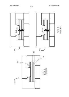
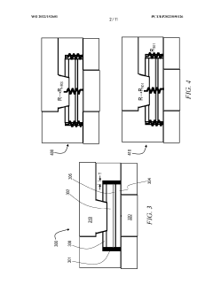
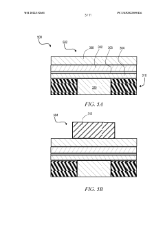
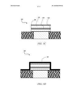
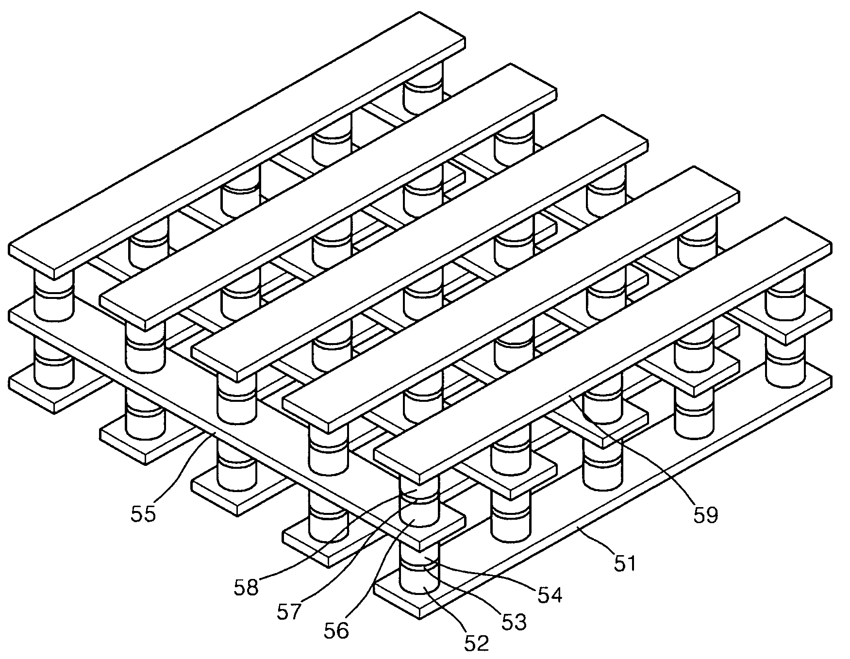
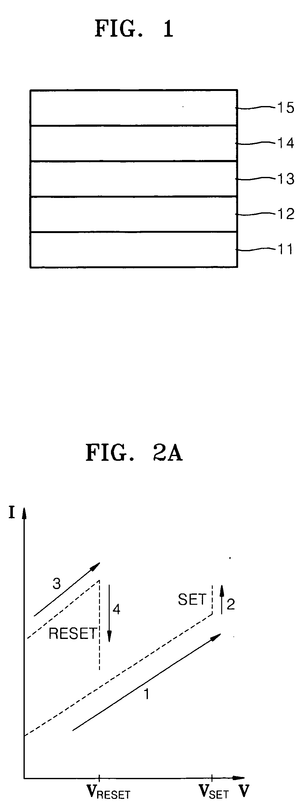
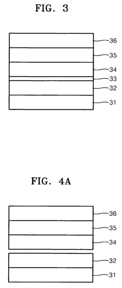
Resistive Random Access Memory (RRAM) devices utilize specific materials and structures to enable resistive switching behavior. These typically include metal oxides like HfO2, TiO2, or Ta2O5 as the switching layer sandwiched between two electrodes. The structure may incorporate additional layers such as barrier layers or doping elements to enhance performance characteristics. Various material combinations and structural configurations are employed to optimize switching speed, endurance, retention, and power consumption of RRAM devices.- Resistive RAM device structures: Resistive RAM (RRAM) devices are constructed with specific structural configurations to optimize performance. These structures typically include a resistive switching layer sandwiched between two electrodes. Various materials can be used for the resistive layer, including metal oxides, chalcogenides, and perovskites. The electrode materials and their interfaces with the resistive layer play crucial roles in determining switching characteristics. Advanced RRAM structures may incorporate additional layers for improved stability, retention, and endurance.
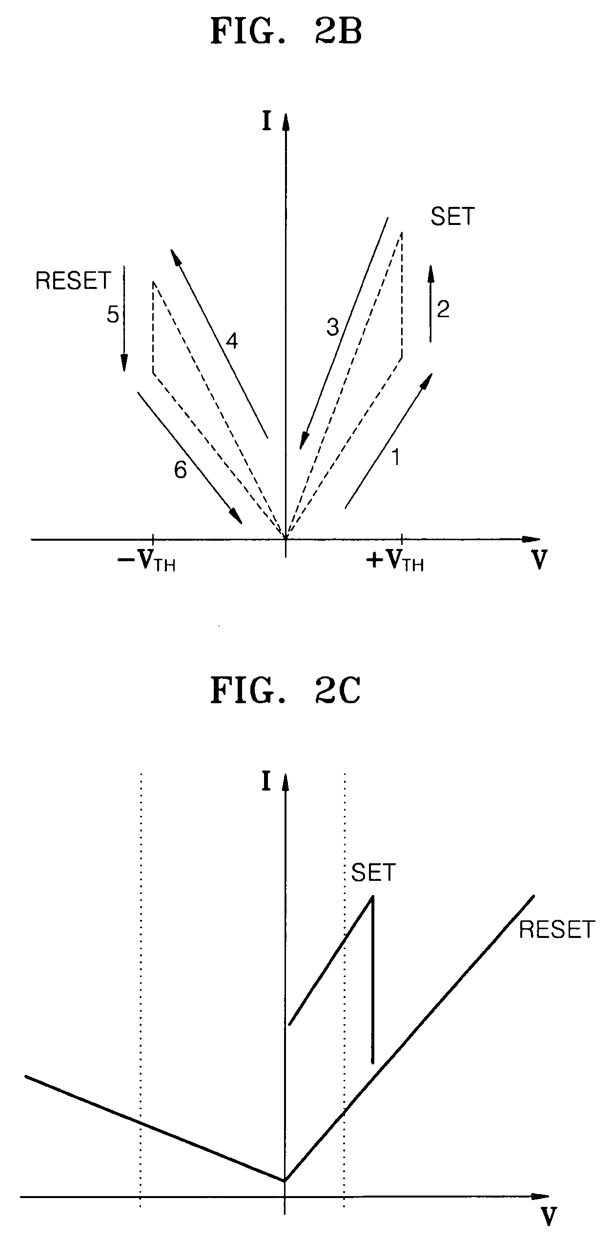
- Resistive switching mechanisms: The operation of resistive RAM relies on various switching mechanisms that change the resistance state of the memory cell. These mechanisms include filamentary conduction, where conductive filaments form and rupture within the resistive layer, and interface-type switching, where the resistance changes at the electrode-oxide interface. Oxygen vacancy migration, ion movement, and phase changes are common physical processes underlying these switching behaviors. Understanding these mechanisms is essential for designing RRAM devices with reliable performance characteristics.
- Integration and fabrication techniques: Fabrication of resistive RAM involves specialized techniques to ensure proper device operation and integration with existing semiconductor technologies. These techniques include precise deposition methods for the resistive switching layer, electrode formation processes, and patterning approaches. RRAM can be integrated into crossbar arrays, 3D stacking architectures, or combined with selector devices to mitigate sneak path issues. Advanced fabrication methods focus on achieving uniformity across large arrays, minimizing cell-to-cell variability, and ensuring compatibility with CMOS processes.
- Operation and control methods: Operating resistive RAM devices requires specific control methods to ensure reliable switching between resistance states. These methods include precise voltage or current application protocols for SET and RESET operations, pulse shaping techniques to optimize switching speed and energy consumption, and verification schemes to confirm successful state changes. Advanced control methods may incorporate adaptive programming algorithms that adjust operating parameters based on device characteristics or implement multi-level cell operation by controlling intermediate resistance states.
- Applications and system integration: Resistive RAM technology finds applications across various computing domains due to its non-volatility, scalability, and compatibility with conventional semiconductor processes. RRAM can be used in storage-class memory, neuromorphic computing systems that mimic brain functionality, in-memory computing architectures, and low-power IoT devices. System-level integration considerations include interface circuits, addressing schemes, error correction mechanisms, and reliability enhancement techniques. The technology's ability to perform both memory and logic functions makes it particularly suitable for emerging computing paradigms.
02 Resistive switching mechanisms
RRAM operation relies on resistive switching mechanisms that allow the device to switch between high and low resistance states. These mechanisms include filament formation/rupture, where conductive filaments form or break within the switching layer, and interface-type switching, where the resistance change occurs at the interface between the electrode and switching layer. The switching can be controlled by voltage polarity (bipolar switching) or voltage amplitude (unipolar switching). Understanding these mechanisms is crucial for designing reliable RRAM devices with consistent performance characteristics.Expand Specific Solutions03 Integration and fabrication techniques
Fabrication of RRAM devices involves various integration techniques compatible with conventional semiconductor manufacturing processes. These include deposition methods such as atomic layer deposition, sputtering, or chemical vapor deposition for the switching layer, and lithography processes for patterning. Integration challenges include ensuring compatibility with CMOS technology, minimizing cell-to-cell variability, and developing reliable 3D stacking approaches. Advanced fabrication techniques focus on reducing feature sizes while maintaining performance and yield.Expand Specific Solutions04 Circuit design and operation
RRAM circuit design encompasses peripheral circuits for programming, reading, and erasing operations. This includes sense amplifiers for detecting resistance states, write drivers for applying appropriate programming voltages, and control logic for managing operations. Circuit techniques address challenges such as sneak path currents in crossbar arrays, read disturbance, and write disturbance. Various programming schemes are implemented to achieve reliable switching between resistance states while minimizing power consumption and maximizing endurance.Expand Specific Solutions05 Applications and emerging technologies
RRAM technology finds applications in non-volatile memory, neuromorphic computing, and in-memory computing. As a non-volatile memory, RRAM offers advantages of high density, low power consumption, and fast switching speed. In neuromorphic applications, RRAM devices can mimic synaptic behavior, enabling hardware implementation of neural networks. Emerging technologies include multi-level cell operation for increased storage density, selector devices for improved array operation, and novel materials for enhanced performance. Research continues to explore RRAM's potential in edge computing and Internet of Things applications.Expand Specific Solutions
Key Industry Players and Competitive Landscape
The Resistive RAM market is currently in a growth phase, with an expanding competitive landscape across multiple industries. Key players like Samsung Electronics, Micron Technology, and Taiwan Semiconductor Manufacturing Co. are driving innovation in this emerging non-volatile memory technology. The market shows varying degrees of maturity across sectors, with consumer electronics leading adoption while automotive and industrial applications are developing rapidly. Technology maturity remains moderate, with companies like IBM, Fujitsu, and Toshiba focusing on overcoming technical challenges related to scalability and endurance. Asian manufacturers, particularly from Taiwan and South Korea, dominate production capacity, while research partnerships between companies like Nantero and academic institutions are accelerating commercialization efforts for next-generation memory solutions.
Taiwan Semiconductor Manufacturing Co., Ltd.
Technical Solution: TSMC has developed an embedded ReRAM (eReRAM) technology specifically optimized for integration with their advanced logic processes. Their approach utilizes a hafnium oxide-based switching layer compatible with their standard CMOS manufacturing flow, enabling seamless integration of non-volatile memory with logic circuits. TSMC's ReRAM implementation features a 1-transistor-1-resistor (1T1R) cell architecture that provides excellent cell isolation and read/write control while maintaining a compact footprint. The company has demonstrated ReRAM arrays manufactured on their 22nm process node with switching speeds below 50ns and endurance exceeding 10^6 cycles. TSMC's market strategy focuses primarily on embedded applications rather than standalone memory, targeting IoT, microcontroller, and edge AI markets where integration of logic and non-volatile memory provides significant system-level benefits. Their ReRAM technology offers particular advantages for ultra-low power applications, with standby power consumption orders of magnitude lower than competing embedded flash solutions. TSMC has established partnerships with multiple IP providers to create standardized ReRAM memory compilers, enabling their customers to easily incorporate ReRAM blocks into system-on-chip designs. The company has reported successful customer tape-outs incorporating their eReRAM technology across multiple application domains.
Strengths: Unparalleled manufacturing expertise and process integration capabilities. Established ecosystem of design tools and IP support enabling rapid customer adoption. Weaknesses: Limited focus on standalone memory markets restricts total addressable market. Current implementations prioritize reliability and integration over raw performance metrics.
Micron Technology, Inc.
Technical Solution: Micron has developed advanced 3D ReRAM (Resistive RAM) technology that combines high-density storage capabilities with low power consumption. Their approach utilizes a cross-point architecture where memory cells are positioned at the intersection of word and bit lines, creating a three-dimensional storage array. This design significantly increases storage density while maintaining fast access times. Micron's ReRAM technology employs oxygen vacancy migration in metal oxide materials to create and dissolve conductive filaments, enabling reliable switching between high and low resistance states. Their implementation includes proprietary selector devices to minimize sneak path currents, a common challenge in cross-point arrays. Micron has demonstrated ReRAM cells with sub-10ns switching speeds and endurance exceeding 10^9 cycles, positioning their technology as a viable Storage Class Memory (SCM) solution bridging the performance gap between DRAM and NAND flash. Their market strategy focuses on enterprise storage systems, data centers, and edge computing applications where ReRAM's combination of speed, endurance, and non-volatility provides significant advantages over conventional memory technologies.
Strengths: Superior performance metrics with fast switching speeds and high endurance compared to competing non-volatile memories. Established manufacturing infrastructure and supply chain integration capabilities. Weaknesses: Higher cost per bit compared to NAND flash limits mass market adoption. Scaling challenges at advanced nodes may impact future competitiveness against emerging memory technologies.
Critical Patents and Technical Innovations in ReRAM
Setting an upper bound on RRAM resistance
PatentWO2022152601A1
Innovation
- Incorporating a high-resistance semiconductive spacer in parallel with the RRAM module, using materials like TiOxNy or TaxNy, to provide an upper bound on resistance, ensuring proper operation even with manufacturing defects and enhancing stability by encapsulating the filament layer.
Resistive random access memory
PatentInactiveUS20090302315A1
Innovation
- A RRAM design that eliminates the need for a diode or transistor structure, using a switch region with bi-polar properties and a memory resistor with uni-polar properties, formed from materials like SiO2, Ni oxides, and a nano bridge with an electrolyte intermediate layer, allowing for variable resistance and efficient data storage.
Cross-Industry Application Scenarios
Resistive RAM (ReRAM) technology demonstrates remarkable versatility across multiple industries, with each sector leveraging its unique advantages to address specific challenges. In the consumer electronics market, ReRAM offers significant potential for next-generation smartphones and tablets, where its low power consumption and high-speed operation can extend battery life while improving device performance. Major manufacturers are exploring ReRAM integration for cache memory applications, potentially revolutionizing mobile computing experiences through faster data access and reduced energy requirements.
The automotive industry represents another promising market for ReRAM deployment, particularly in advanced driver-assistance systems (ADAS) and autonomous vehicles. These applications demand memory solutions capable of rapid data processing in harsh environmental conditions—requirements that ReRAM meets through its radiation hardness, temperature stability, and quick read/write cycles. As vehicles become increasingly computerized, ReRAM could become essential for real-time decision-making systems where reliability is paramount.
In industrial automation and IoT applications, ReRAM's non-volatility and endurance characteristics make it particularly valuable for edge computing devices operating in remote or challenging environments. The technology enables persistent local storage with minimal power requirements, allowing sensors and controllers to maintain critical data even during power interruptions. This capability is driving adoption in smart manufacturing systems, utility infrastructure monitoring, and other industrial applications where system resilience is essential.
The healthcare sector presents unique opportunities for ReRAM implementation, particularly in medical imaging equipment and implantable devices. The technology's combination of high density, low power consumption, and radiation resistance makes it suitable for portable diagnostic tools and long-term implantable monitors. Several medical device manufacturers are investigating ReRAM for next-generation equipment where reliability and energy efficiency directly impact patient outcomes.
Aerospace and defense applications represent a premium market segment for ReRAM, where its inherent radiation hardness provides significant advantages over conventional memory technologies. Satellite systems, military communications equipment, and avionics can benefit from ReRAM's ability to maintain data integrity in high-radiation environments while consuming minimal power—critical factors for space-based and defense applications where maintenance is difficult or impossible.
Supply Chain and Manufacturing Considerations
The supply chain for Resistive RAM (ReRAM) presents unique challenges and opportunities that significantly impact its market adoption across different industries. Manufacturing ReRAM requires specialized equipment and processes, with key components including metal oxide materials, electrode metals, and integration materials. The supply chain currently faces concentration risks, as critical raw materials like hafnium, tantalum, and certain transition metals are sourced from limited geographical regions, creating potential vulnerabilities to geopolitical tensions and trade restrictions.
Production scalability remains a significant hurdle for ReRAM manufacturers. While the technology theoretically offers manufacturing advantages over NAND flash, including fewer mask layers and potentially simpler process steps, achieving consistent yield rates at high volume has proven challenging. Leading manufacturers have reported variable yields between 60-85%, compared to the 90%+ consistently achieved in mature NAND flash production lines. This yield gap directly impacts unit economics and market competitiveness.
Manufacturing partnerships have emerged as a critical strategy in the ReRAM ecosystem. Pure-play foundries like TSMC, GlobalFoundries, and UMC have developed specialized ReRAM process nodes, while IDMs such as Micron and Samsung integrate ReRAM production into their existing memory fabrication infrastructure. These partnerships create different supply chain dynamics across application segments, with embedded ReRAM benefiting from integration with standard CMOS processes, while standalone ReRAM products require dedicated production lines.
Cost structures for ReRAM manufacturing vary significantly by application and scale. Current cost analyses indicate that at volumes below 10,000 wafers monthly, ReRAM production costs remain 30-40% higher than equivalent NAND capacity. However, as production scales beyond this threshold, the gap narrows to 10-15%, making ReRAM increasingly competitive for specialized applications. The industry anticipates reaching cost parity with NAND in specific application segments by 2025-2026, particularly for industrial and automotive use cases where ReRAM's endurance and temperature performance justify premium pricing.
Sustainability considerations are increasingly influencing ReRAM supply chain development. The technology offers potential environmental advantages over conventional memory technologies, including lower energy consumption during manufacturing and reduced use of certain toxic chemicals. However, the industry must address emerging concerns about the recyclability of metal oxide materials and potential resource constraints for certain electrode metals as production volumes increase.
Unlock deeper insights with Patsnap Eureka Quick Research — get a full tech report to explore trends and direct your research. Try now!
Generate Your Research Report Instantly with AI Agent
Supercharge your innovation with Patsnap Eureka AI Agent Platform!